افشین رشید
اُستادیار ؛ عضو هیات علمی دانشگاه آزاد اسلامی واحد علوم و تحقیقات تهران
651 یادداشت منتشر شدهnMOS Transistor ( With Negative Resistance Region ) and Voltage Control Capability
Note: The nMOS or programmable transistor is made up of four P and N type semiconductor pieces. The bases of an nMOS transistor are called Anode, Gate and Cathode.
This element also has a negative resistance region like the UJT transistor. Therefore, we can use it in oscillators or thyristor control circuits. Choosing the name nMOS , which means programmable UJT, was chosen because of the controllability of the voltage value, because in the nMOS transistor , the voltage value can be programmed or set to any desired value. The nMOS transistor is a controllable transistor, so we can use it to adjust the voltage to the desired value.
The nMOS element is widely used in circuits such as oscillators and timers. The nMOS transistor has a four-layer structure just like thyristors and has three terminals called anode (A), cathode (K) and gate (G) again like thyristors. This transistor is called programmable only because its characteristics and parameters are very similar to single-function transistors. This is planning.
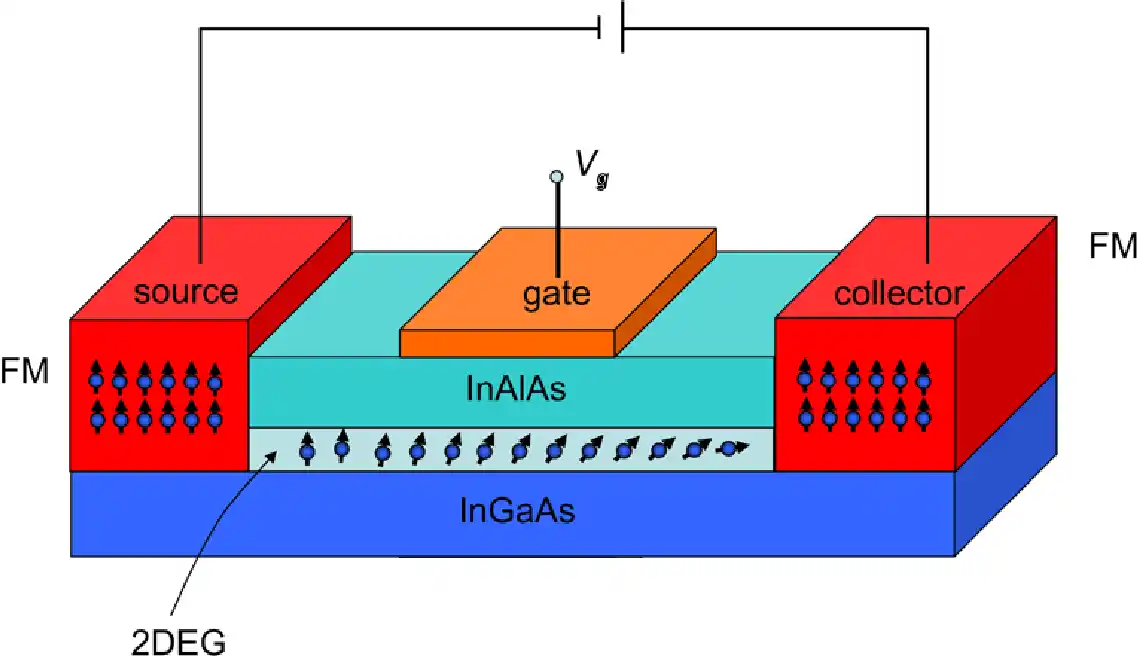
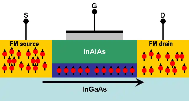
nMOS transistors are very useful in amplifiers because of their nearly infinite input impedance, which allows the amplifier to capture almost any input signal. The main advantage is that it requires almost no input current to control the load current, compared to bipolar transistors. Field effect transistor ( nMOS ) is considered with three bases called gate, drain, and source. In this transistor, the gate (control base) does not draw current, and as the name of the transistor suggests, the current passing through the nMOS is controlled only by applying voltage and creating an electric field inside the semiconductor . Therefore, when the gate is considered as the input of this transistor, it does not have any loading effect on its previous stages in the circuit, and the transistor has a very high input impedance in this state. The main difference between MOSFET and other transistors is that the gate of MOSFET transistors is separated from the channel by a layer of silicon oxide (SiO
2 ).