افشین رشید
اُستادیار ؛ عضو هیات علمی دانشگاه آزاد اسلامی واحد علوم و تحقیقات تهران
384 یادداشت منتشر شدهIn Nanoelectronics Technology, Sublayer Surface Processes (Si and Gi) Such as Burning Are Carried Out by Plasma and ion Beam Technology

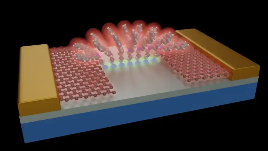
Note: In nanoelectronics technology, sublayer surface processes (Si and Gi) such as burning are carried out by plasma and ion beam technology. Such integrated circuits with their unique characteristics on the nanometer scale have various applications of (mesoscopic) systems.
Characterization of multi-layer Si/Gi systems recently exists in the field of the effect of negative bias voltage on the improvement of the nanoelectrical and structural properties of the permeation barrier of the Ta sputtering layer in the nano Si/Ta system. Also, in the technology of designing nano-electronic parts by using and manufacturing the thin layers required in the mentioned integrated circuits only in the environments defined by precise deposition methods such as molecular beam deposition (MBE) and organic metal chemical vapor deposition (MOCVD). ) It is possible.

Basically, semiconductor-metal connections are a necessary part of all nanoelectronic components. How and the behavior of nano electrical connections depends on the concentration of the semiconductor (Si) and (Gi) surface, the cleanliness of the surface and the reactions between the metal-semiconductor interface. After the invention of nano transistor, the concept and importance of integrated circuits became clear. After that, the great success of assembling and connecting a large number of small parts and electronic components on the substrate surface caused a huge evolution in the practical construction of integrated circuits. With the development and development of the miniaturization technology of nano-microelectronic parts, the use of quantum tunneling nano systems in resonator nano diodes (Si and Gi) and other nano parts is possible. With the expansion, the design and manufacture of integrated nano circuits, especially the increase in the accumulation of components on a very large scale, and efforts to make microelectronic components smaller continued. On the other hand, the new demand for the construction of integrated circuits, especially memory nano circuits, including dynamic nano memory (DRAM) and static memory (SRAM) with features such as high operating speed and reduced power loss, increased day by day . In the evolutionary process of ultra-miniaturization technology of electronic nano parts, especially in geometry and sub-micron scale of less than 2.0 micrometers, i.e., the field of nano electronic parts design technology and manufacturing technology based on Gi and Si nano structures of nano integrated circuits has a special complexity.
Conclusion :
In nanoelectronics technology, sublayer surface processes (Si and Gi) such as burning are carried out by plasma and ion beam technology. Such integrated circuits with their unique characteristics on the nanometer scale have various applications of (mesoscopic) systems.