افشین رشید
اُستادیار ؛ عضو هیات علمی دانشگاه آزاد اسلامی واحد علوم و تحقیقات تهران
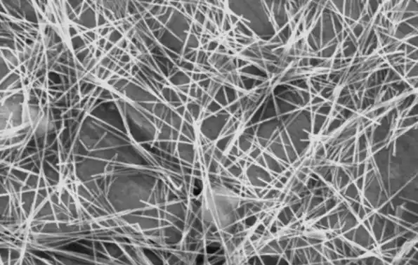
762 یادداشت منتشر شدهNanowires (NWS) Doped nano wire

Note: Nanowires (NWS) alone cannot control the movement of electrons, so the impurity must be ina process called Doping, usually added with boron, phosphorus, selenium or germanium.
When the nano wire is doped, the electron movement can be converted and allows electron flow, or off (stopping the flow of electrons), using the interlayer voltage of nanowires (NWs) on and turns off. Another nanostructure that has received many studies and researches today is nanowires. Generally, the wire is said to be a structure that is extended in one direction (longitudinal direction) and is very limited in the other two directions . A basic feature of these structures that have two outputs is electrical conductivity. By applying an electric potential difference at the two ends of these structures and along their length, electric charge transfer occurs. Making wires in nanometer dimensions both technologically and It is very interesting from a scientific point of view, because it exhibits unusual properties in nanometer dimensions. The ratio of length to diameter of nanowires is very high (metal nanowires). ) these nanostructures promise great efficiency in electronic components due to their special properties. Metal nanowires are one of the most attractive materials due to their unique properties that lead to their various applications. a i=16> are. Nanowires can be used in computers and other computing devices. To achieve complex nanoscale electronic components, we need nanoscale wires. In addition, nanowires themselves can be the basis of electronic components such as memory.
(Organic nanowires) This type of nanowires, as their name implies, are obtained from organic compounds. It is possible. Recently, a material called "oligophenylene vinyline" has been considered for this purpose. The properties of these wires (such as conductivity, resistance, and thermal conductivity) are It depends on the structure of the monomer and its arrangement.The chemical structure of these compounds creates interesting properties. The future of nanotechnology depends on the ability of researchers to achieve the techniques of organizing molecular components and achieving nanometer structures. By imitating nature, achieve the organization of proteins from yeast to produce conductive nanowires. Organizing living components in nature is the best and oldest example of "bottom-up" construction, and therefore it can be used to understand and also find methods for making electronic devices. and used a micrometer. Until now, "top-down" manufacturing techniques were used, which are often laborious and expensive at the nanometer scale, and the commercialization of nanotechnology requires easy and affordable methods that are the best. a> This type of nanowires has shown its greatest use in the field of medicine, such as detecting signs of cancer, growth of stem cells, etc., which we will discuss below. (Silicon nanowires) This type of nanowires is not toxic and does not harm the cells. its pattern is the nature around us; It is enough to open our eyes a little and look more carefully around us.
Conclusion :
Nanowires (NWS) alone cannot control the movement of electrons, so the impurity must be ina process called doping. Usually added with boron, phosphorus, selenium or germanium.