افشین رشید
اُستادیار ؛ عضو هیات علمی دانشگاه آزاد اسلامی واحد علوم و تحقیقات تهران
651 یادداشت منتشر شدهflexible multi-dimensional (electronic) nanostructures sTMD in nanometer dimensions
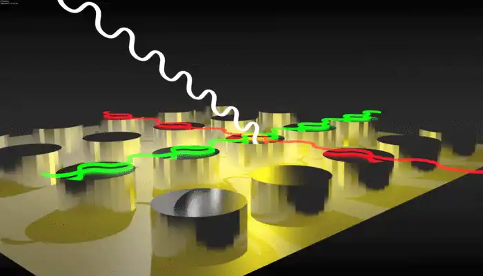
Note: Features of flexible multidimensional materials sTMD in nano dimensions Modern semiconductors have revolutionized a wide range of technologies such as electronics, lighting, solar energy, and communications.
Most nanometals and metal nanoalloys, semiconductors, ceramics and some nanopolymers that have a crystalline structure have long-range order in their structure. The extent of this order between atoms or ions should be more than 100 nm. Atoms or ions are regularly repeated in three dimensions. Materials with long-range order are called crystalline materials. If a material has one large crystal, it is called a single crystal material. Single crystal materials are suitable for many electronic and optical applications, for example, computer chips are made of single crystal silicon. Polycrystalline material consists of many small crystals in three dimensions. Monolayers are classified into H or T structures according to their stability, where H is the most common structure with TMD symmetry and trigonometric prismatic metal coordination, and T indicates a structure with multiple symmetry. Dimension and coordination of metals is octagonal and are unstable structures.
In particular, single-layer TMDs of the multidimensional nanogroup are direct-gap semiconductors, while their bilayers and thicker multilayers have indirect gaps. for example flexible multidimensional materials sTMD in nano dimensions a> Electronic structure all when passing from two layers to one cross layer from indirect to direct gap. In general
Conclusion :
The nano-microelectronics industry uses Si to make electronic circuits and GaAs, GaN, and other III-V materials for optical nanodevices, with typical substrates consisting of manufactured wafers. =1>flexible multidimensional materialssTMD in nano dimensions at high temperature. Precisely controlled thin films can be deposited on the substrate to achieve additional functionalities, for example by chemical vapor deposition (CVD) or molecular beam epitaxy.