افشین رشید
اُستادیار ؛ عضو هیات علمی دانشگاه آزاد اسلامی واحد علوم و تحقیقات تهران
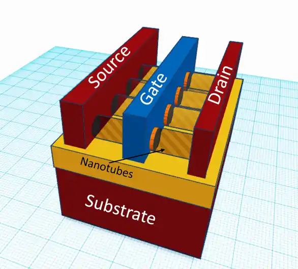
651 یادداشت منتشر شده(Field effect nano transistors) Nano transistor Electronic quantity and ionization potential
Note: In the structure of (Nano transistors) the electronic quantity that is more easily available is the ionization potential and in the potential Ionization is more in the size of small grains of the nanostructure (smaller particles), that is, with the increase in the size of the particles, their ionization potential decreases.
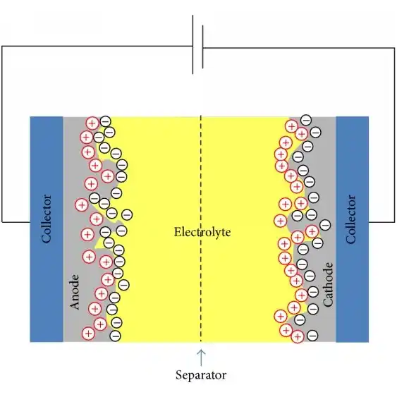
increasing the ratio of surface to volume and changes in geometry and electronic structure have a strong effect on the chemical interactions of matter, and for example, the activity of small particles with change It changes in the number of atoms (and thus the size of the particles).Unlike today's nanotransistors, which behave based on the movement of a mass of electrons in matter, the new devices are based on the phenomena of quantum mechanics. At the nano scale, the discrete nature of the electron cannot be ignored anymore.By reducing all the horizontal and vertical dimensions of the transistor, the electric charge density in different areas of the nano transistor increases, or in other words, the number of electric charges per unit area of the nano-transistor increases.
This incident has two negative consequences :
First, with the increase of the electric charge density, the possibility of discharging the electric charge from the insulating areas of the transistor increases and this event causes damage to the transistor and its failure. This event is similar to the discharge of excess electric charge between the cloud and the ground in the phenomenon of lightning, which causes air molecules to ionize into negative and positive ions. . Secondly With the increase of the electric charge density, electrons may leave the range of the radius of one atom under the influence of repulsive or abduction forces which have now increased in value and enter the radius range of the adjacent atom. This event is called tunneling in quantum physics. Electron tunneling from one atom to the adjacent atom is a phenomenon that happens a lot in small dimensions between electrons. This phenomenon is the basis of the work of some electronic components and some nanoscopes. But in nanotransistor, this phenomenon is not a useful phenomenon, because electron tunneling from one atom to the adjacent atom may continue and an electric current Shrinking transistors and entering dimensions below 100 nanometers in the performance range of nanoelectronics technology, although it has many advantages but with challenges diversity is faced. Designing, manufacturing, developing and using products whose size is in the range of 1 nm a> . And this trend has been noticed in the production of Nano transistors. 100 are called nanoelectronics. In fact, we are talking about miniaturization, which allows for more contact, more activity, and an increase in area. Nano is a new scale in technologies and a new approach in all disciplines, and it gives mankind the ability to expand its involvement in the structure of materials and design and manufacture in very small dimensions and in all technologies. that mankind has already achieved, to have an effectnm to
Conclusion :
In the structure ( Nano transistors) Nano transistor The electronic quantity that is more easily accessible is the ionization potential and in the ionization potential in The size of small grains of the nanostructure (smaller particles) is more, that is, with the increase in the size of the particles, their ionization potential decreases.