افشین رشید
اُستادیار ؛ عضو هیات علمی دانشگاه آزاد اسلامی واحد علوم و تحقیقات تهران
654 یادداشت منتشر شدهA combination of interference nanolithography and nanoelectronics lithography enables the fabrication and reproduction of high-resolution structures in large areas
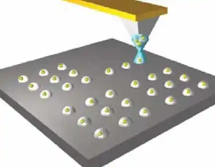
Note: Micro- and nano-structures can be used to reduce reflection or guide light in applications such as photovoltaic solar cells, LEDs, or nanoelectronics technology.
Electron beam lithography provides the possibility of precise control of nanostructure characteristics that form the basis of various nanotechnologies. The nanostructure fabrication and measurement group advances lithography precision at the nanometer scale and creates processes for manufacturing innovative devices and standards in physical fields ranging from photonics to fluids.< /span>Such measurements create a positive feedback loop for the fabrication and measurement of nanostructures.Electron beam lithography is used for pattern standards for atomic force correlation microscopy and ultra-resolution optical microscopy, with high-throughput precision localization and process parameter characterization and optimization. To improve pattern placement, To reduce the entry barrier of electron beam lithography and to improve control of pattern accuracy, the nanolithography toolbox is also used, to advance fundamental capabilities in electron beam lithography, and developing methods to better control, measure, and understand manufacturing processes is. optical microscopy standards for aberration correction and Ultraviolet to infrared levels for trapping and probing atoms and ions, polarimetry, imaging and superfast space-time laser pulse shaping. Quantum photonic integrated circuits with nonlinear and quantum light sources for quantum information. optical mechanical and micro/nanoelectromechanical systems on cavity for sensing, transmission and nonlinear dynamics studies; Integrated nonlinear optics for quantum wavelength and frequency conversion. and However, achieving these performance criteria is dependent on interrelated factors that are sample-specific—pattern definition and breakdown, substrate and mask materials, pre- and post-exposure processes. Exposure is the definition of the alignment feature—and also, importantly, the performance details of the lithography system. As a core capability, we develop processes that are at or near the limits of conventional electron beam lithography. are to advance nanoscale devices and measurement science in various fields, such as: chip-scale frequency combs for accurate timekeeping; Lateral resolution of 10nm, placement accuracy of 1nm and patterning areas of 1mm are all possible. Electron beam nanolithography provides the possibility of precise control of nanostructure features that form the basis of various device technologies.

The ability to produce large micro and nanostructures on non-planar surfaces is important for many applications such as optics, optoelectronics, nanophotonics, imaging technology, NEMS and microfluidics.With this Now, it is very difficult to create large nanostructures on curved or non-planar surfaces using existing patterning methods. Furthermore, a variety of current nanopatterning technologies, such as electron beam lithography, optical lithography, interference lithography (IL), etc., cannot meet all the practical demands of industrial applications in terms of high resolution. High power, low cost cope. , large area and patterns on non-flat and curved surface. Therefore, new high-volume nano-manufacturing technology urgently needs to be exploited and developed to meet the extraordinary needs of growing markets.Lithography Nanoelectronics is currently considered as a promising low-cost, high-throughput, and high-resolution nanopatterning method, especially for the production of large-scale small/nanopatterns and complex 3D structures, as well as the aspect The above characteristics of the ratio regarding these outstanding advantages have also resulted. This field becomes Especially, nanoelectronic lithography has great potential to set new standards for making miniature, low-cost and light-weight optics that can be used in many fields of applications.

Conclusion :
Micro- and nano-structures can be used to reduce reflection or guide light in applications such as photovoltaic solar cells, LEDs, or nanoelectronics technology.