افشین رشید
اُستادیار ؛ عضو هیات علمی دانشگاه آزاد اسلامی واحد علوم و تحقیقات تهران
657 یادداشت منتشر شدهScanning Nano Lithography) or Nano Lithography)
Note: Scanning Nano Lithography or Scanning Nano Lithography enables the original or improved nano pattern in applied fields ranging from quantum technologies to material science.
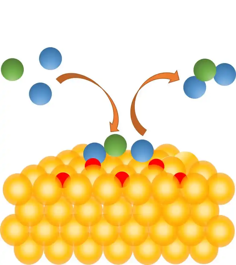
In particular, ultra-fast and highly localized thermal processing of surfaces can be achieved through a sharp heating tip to create high-resolution patterns. Many possible applications of nanoscale modifications with thermal probes such as Scanning Nano Lithography are still applicable in nanoelectronics, especially when which can use extremely high heating and cooling rates.Many microsystems and nanosystems require precise nanoscale patterns that exhibit intrinsic functionality, such as some electronic properties. , photonic, chemical and mechanical. To make these nanoscale patterns, electron beam lithography is the most common lithography technique without direct writing and without mask.Scanning Nano Lithography A complex electron compatible optic is required to focus the electron beam into a spot of a few nanometers. Another issue is electron scattering, a kind of proximity effect, on the surface of the sample, which leads to the exposure of additional undesirable resistivity that must be corrected by intensive calculation algorithms. Scanning Nano Lithography is another method of direct writing nanolithography, where patterns are created by scanning a nanometer tip on the sample to create local changes. Sample-sample interactions are numerous and can include mechanical, electrical, diffusion, and thermal effects.
Since nano-optical devices are produced using wafer-based processes that are used in semiconductor manufacturing, this allows for flexible sharing of production capacity and allows production capacity to be shared with High volume support. Some materials can create regular, nanoscale structures under appropriate and controlled conditions - self-assembly. The problem of this approach is the lack of flexibility in the structures that can be achieved and the materials that can be used, which limits the functions that can be realized. The advantages of this technique can be He mentioned the wide patterns, simplicity, good resolution and ability to combine with other lithographic techniques. On the other hand, this technique creates problems due to the limited forms available for patterned functional materials, the arrangement of nanopatterns and the presence of point defects.

Conclusion :
Scanning Nano Lithography enables original or improved nano-patterning in applications ranging from quantum technologies to materials science.