افشین رشید
اُستادیار ؛ عضو هیات علمی دانشگاه آزاد اسلامی واحد علوم و تحقیقات تهران
651 یادداشت منتشر شدهHigh-speed plasmonic nanolithography with half-step resolution (۲۲ nm)
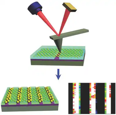
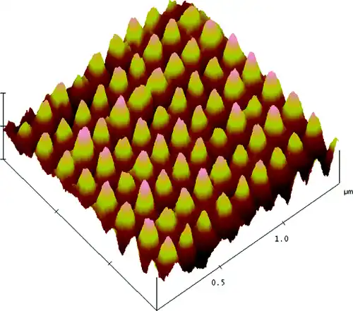
Note: high-speed plasmonic nanolithography with a half-step resolution of 22 nm using multi-stage plasmon focusing through relatively low-emission surface plasmons focused and later to Localized plasmons are converted. This allows for highly efficient transmission and near-field spot focusing, which is key to improving power, for a given laser power, by increasing the scan speed and/or using the number of parallel patterns. slow
Basically, high-speed plasmonic nanolithography with half-pitch resolution (22 nm) allows us to produce nanoelectronic devices that can create 12-inch wafers in minutes. This is comparable to conventional photolithography at the production level but at a much higher resolution than the 22 nm half-pitch size. This new design enables low-cost, high-efficiency maskless nanoscale fabrication with several orders of magnitude higher throughput than conventional maskless methods. Using shorter wavelength plasmonic nanolithography and conduction mechanisms, it may achieve continuous scaling down to node sizes smaller than 22 nm, providing a promising path for next-generation lithography to produce open semiconductors. slow Furthermore, next-generation magnetic data storage, known as heat-assisted nanoelectronic devices and nanobit-patterned media, has great potential in the future. have twice the capacity.
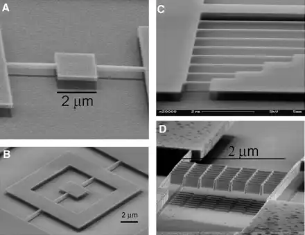
The application of nanolithography is the manufacture of integrated circuits and other electronic devices, where optical lithography is widespread. In addition, various types of nanolithography techniques are used in research activities with the aim of modeling materials and realizing prototypes and proof-of-concept devices. Methods of applying nanolithography on a spin substrate according to the specific interactions between these polymers and the substrate, in Under certain conditions, two types of polymers tend to form interwoven patterns, there is a local order between both polymers, and it forms nanowire-like domains with a period in the range of 50 nm. This pattern will be very useful if the subsequent application of nanolithography , which after landing on the layer due to lower penetration mobility, It tends to accumulate on top of the polymer. Thus, it follows the thin underlying structure of the polymer scaffold, which extends undisturbed over several microns. However, the formed nanowires reveal some unwanted features as a closer look reveals possible roughness. Attention is observed in the fabrication of nanowires, also the nanowires are interrupted at certain points and deviate from the straight shape, all of which are usually the origin of the deterioration of the physical properties of the nanowires. Furthermore, long-range ordering of nanowire arrays fabricated following this strategy is not achieved, which is essential in certain applications such as semiconductor industries.
Conclusion :
High-speed plasmonic nanolithography with a half-step resolution of 22 nm using multi-stage plasmon focusing through relatively low-emission surface plasmons and later focused to plasmons It becomes local. This allows for highly efficient transmission and near-field spot focusing, which is key to improving power, for a given laser power, by increasing the scan speed and/or using the number of parallel patterns. slow