افشین رشید
اُستادیار ؛ عضو هیات علمی دانشگاه آزاد اسلامی واحد علوم و تحقیقات تهران
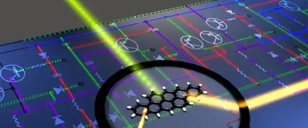
657 یادداشت منتشر شدهNanolithography Focused Ion Beam or (FIB) (below ۱۰۰ nm - ۱۰ nm range) in the manufacture of nanoelectronic devices
Note: Accelerated ion collisions are very suitable for sputtering atoms on the surface of materials for recreational lithography. Thanks to the development of the technology of producing focused ion beams in ion microscopes, this method has become a nanolithography technique with very high lateral resolution in the sub-10 nm range.
sources of focused ion beam nanolithography due to its stability and ease of use it was mainly based on nanotechnology , scanning focused ion beam on the surface of a material removes materials with the desired pattern and with high nanoscale accuracy, and for The conceptual design of nanolithography uses a focused ion beam and integrates similar components: sources, extraction and acceleration, optics, scan coils, sample stage, electron detectors, etc. Interestingly, the focused ion beam nanolithography equipment provides the user with all imaging, nanostructural and analysis capabilities of both technologies in a single platform. For this reason, focused ion beam technology has become very popular for performing specific tasks such as cross-sectional imaging, preparation of nanodevice layers, nanopatterning of materials, and circuit editing.
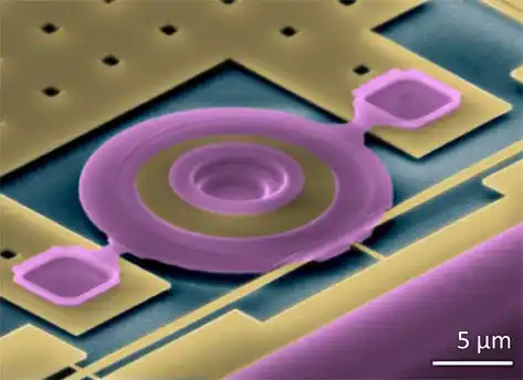
Focused ion beam nanolithography is able to directly remove materials without using a lot of resistors. As a direct nanolithography method, the number of processing steps is minimized compared to other methods.Focused ion beam nanolithography As a sequential nanolithography technique, it is inherently slow and its throughput is much lower than other techniques and Liquid metal ion source based Ga + is the most widespread source type in focused ion beam nanolithography equipment has been converted. However, in recent years, new developments in sources such as gas field ion sources, plasma sources and Metal alloy sources are the next step in terms of clarity or power. Since the ion-matter interaction is stronger than the electron-matter, harmful effects can be created on the remaining material and the physical properties and changed it chemically. Important but key applications for focused ion beam nanolithography technology in the semiconductor industry has been found in nanotechnology and in materials science. And deposition caused by focused ion beam nanolithography The gas injection system needs to produce a local deposition from a precursor material that is delivered in gaseous form, with the separation of the precursor created by appropriate radiation in nanoelectrical devices. The main advantage of this technique is the selective growth of a material in the region of interest in one step. Due to the high resolution of the focused ion beam nanolithography technique , deposits can be grown with high lateral resolution< /span>focused ion beam nanolithography.On the other hand, the growth rate and metal content of the deposits are generally used for , but due to much less damage caused to the substrate due to the lower linear motion of electrons compared to ions.
Conclusion :
The ability of accelerated ion collisions to splatter atoms on the surface of materials is very suitable for recreational lithography. Thanks to the development of the technology of producing focused ion beams in ion microscopes, this method has become a nanolithography technique with very high lateral resolution in the sub-10 nm range.