افشین رشید
اُستادیار ؛ عضو هیات علمی دانشگاه آزاد اسلامی واحد علوم و تحقیقات تهران
504 یادداشت منتشر شدهUV interference nanolithography (optical nano-electronics)
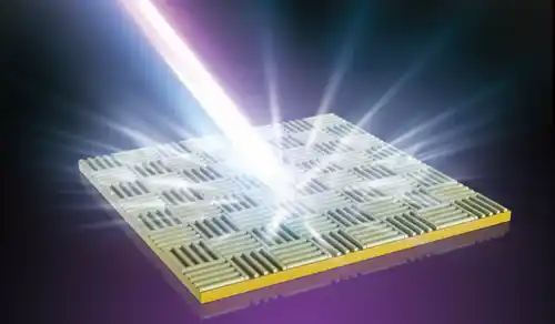
Note: to easily create interference patterns of useful dimensions using UV light sources. The advantage of this method is simplicity. The problem is in creating complex shapes and arrays.
Nanolithography is a branch of nanotechnology that deals with the study and application of fabricating structures at the nanometer scale—meaning the creation of patterns with at least one lateral dimension between the size of an individual atom and approximately 100 nanometers. It is used in the fabrication of advanced semiconductor integrated circuits (nanocircuits) or nanoelectromechanical systems (NEMS).Nanolithography is a broad term. To describe different processes for creating nanoscale patterns in different environments, the most common of which is silicon semiconductor material. The dominant goal of nanolithography is the miniaturization of electronic devices, which allows more electronic components to be packed into smaller spaces, i.e. smaller integrated circuits, which leads to smaller devices, because they are produced faster and cheaper. Because less material is needed. This also increases performance and response time because electrons only have to travel very short distances.
The ability to produce large micro and nanostructures on non-planar surfaces is important for many applications such as optics, optoelectronics, nanophotonics, imaging technology, NEMS and microfluidics.With this Now, it is very difficult to create large nanostructures on curved or non-planar surfaces using existing patterning methods. Furthermore, a variety of current nanopatterning technologies, such as electron beam lithography (ELB), optical lithography, interference lithography (IL), etc., cannot meet all the practical demands of industrial applications in terms of resolution. High, high power, low cost cope. , large area and patterns on non-flat and curved surface. Therefore, new high-volume nano-manufacturing technology urgently needs to be exploited and developed to meet the extraordinary needs of growing markets.Lithography Nanoelectronics is currently considered as a promising low-cost, high-throughput, and high-resolution nanopatterning method, especially for the production of large-scale small/nanopatterns and complex 3D structures, as well as the aspect The above characteristics of the ratio regarding these outstanding advantages have also resulted. This field becomes Especially, nanoelectronic lithography has great potential to set new standards for making miniature, low-cost and light-weight optics that can be used in many fields of applications.
Conclusion :
to Easily creates interference patterns of useful dimensions using UV light sources. The advantage of this method is simplicity. The problem is in creating complex shapes and arrays.