افشین رشید
اُستادیار ؛ عضو هیات علمی دانشگاه آزاد اسلامی واحد علوم و تحقیقات تهران
663 یادداشت منتشر شدهA Complete Explanation of The (Compound Supply) Bias Divider Voltage in nMOs Field Effect Transistors
Note: However, in the "internal self-powered" method, creating negative feedback to some extent stabilizes the bias divider voltage in the operation of the nMOs field effect transistor.
But if we want the circuit to have the highest stability point, we use a circuit according to the bias divider voltage. In this circuit, the voltage divider bias of the nMOs field effect transistor and the self-power circuit (internal resistance) are used simultaneously. For this reason, this power supply is also called a compound power supply. Given that no current flows through the gate of the transistor, the gate voltage is equal to the potential drop across the source and drain in the nMOs field effect transistor. In other words, the voltage at the gate is divided between the source and drain , and the electric potential is obtained at the source and drain . Since this voltage is positive, in order for the gate voltage in the nMOs field effect transistor to become negative, the source potential must be greater than the drain so that the gate-source junction is in the opposite bias.

The resistive voltage can also be obtained by using a transfer curve such as the self-bias plot analysis in the operating characteristic through the resistive voltage. In this plot, the load line on the characteristic curve in the nMOs field effect transistor is not zero because the bias type resistors create a potential drop in the gate at the voltage point. Therefore, in the divider of this circuit, the DC load line passes from the origin of the coordinates, that is, from a point in the load line loop, the DC voltage in the transistor structure in the nMOs field effect transistor does not enter the circuit.
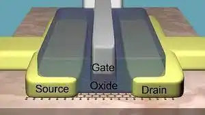
To create a suitable operating point, we must bias the nMOs field effect transistor as well as the nMOs field effect transistor. The biasing methods for the nMOs field effect transistor are not fundamentally different from the BJT biasing methods; it should only be noted that because the input resistance in the nMOs field effect transistor is very high, very little current (about a few nanoamperes or picoamperes) flows through the gate, which can be ignored. In the calculations, the nMOs field effect transistor is taken to be equal to zero. This simplifies the calculations. The simplest method of biasing the nMOs field effect transistor is to use two separate voltage sources, which are used for (drain and gate). This method is called biasing with constant supply voltages.
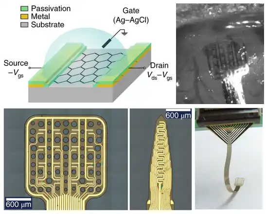
Study and Analysis of Nanotransistors (Graphene - Full Carbon) Graphene Nanotransistors Structure and Function
Investigation of The Self-organized Electrical Nanostructure DND and The influence of Nanoelectromagnetic interactions on The Energy Characteristics of Nanoelectrons (Nanostructures)