افشین رشید
اُستادیار ؛ عضو هیات علمی دانشگاه آزاد اسلامی واحد علوم و تحقیقات تهران
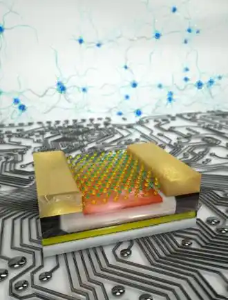
651 یادداشت منتشر شدهIn The Circuit Diagram of a Multilayer Si Graphene Field Effect (Nanotransistor), The Two Source and Drain Electrodes are Directly Connected To The Semiconductor
Note: Graphene, which is made up of just one carbon atom, can be used to create multilayer graphene field-effect nanotransistors that consume less energy and take up less space.
Graphene is a zero-gap semiconductor material that is unsuitable for logic circuits, but nanotechnology has been used to create different forms of the material with different gaps. Graphene nanoribbons, multilayer graphene, and graphene grown on Si are examples of these forms. The term nanotransistor is a combination of the words nanoscale in transmission and resistance. In a Si graphene field effect nanotransistor, the resistance between two electrodes can be switched or controlled by a third electrode. In a Si multilayer graphene field effect nanotransistor, the current between the two electrodes is controlled by the electric field from the third electrode. In contrast, in a bipolar transistor, the third electrode is capacitively connected and is not in contact with the semiconductor. The three electrodes in the Si multilayer graphene field effect nanotransistor structure are connected to the source, drain, and gate.
In the circuit diagram of a multilayer Si graphene nano-field effect transistor, the two source and drain electrodes are directly connected to the semiconductor, while the gate electrode is capacitively connected to the semiconductor using a gate dielectric. The electric field created by the gate electrode controls the current created by the two source and drain electrodes. The drain current is modulated by changing the density of charge carriers in the two-dimensional transmission channel. In a multilayer Si graphene nano-field effect transistor, the drain current is modulated by the thickness of the three-dimensional transmission channel. Numerous chemical and physical methods have been proposed to produce different types of multilayer nano-graphene. The basic principle of physical methods is that these methods try to eliminate the forces between the graphene sheets in graphite and separate them to reach single layers of graphene or graphene oxide, which is the same as the top-down method. In chemical methods, multilayer nanographene is made by placing individual carbon atoms together, which is also called the bottom-up method. In the multilayer nanographene exfoliation method, the electronic quality of the layers is high, the cost of producing graphene in this method is low and does not require special equipment. In field-effect nanotransistors using graphene (Si), the number of nanographene layers produced by this method is single and multilayer. One of the limitations of using this method is that it is not suitable for bulk production and the thin layers produced are non-uniform and uneven, and it is a time-consuming method.
Conclusion :
Graphene, which is made up of just one carbon atom, can be used to create multilayer graphene field-effect nanotransistors that consume less energy and take up less space.