افشین رشید
اُستادیار ؛ عضو هیات علمی دانشگاه آزاد اسلامی واحد علوم و تحقیقات تهران
651 یادداشت منتشر شدهMicro -Structured Nanowire Filaments and Cylinders (Silicon/Germanium) for Possible Applications in Electronic Energy

Note: Fine filaments and cylinders of structured nanowires (silicon/germanium) are used for possible applications in energy, electronics, optics, and other fields.
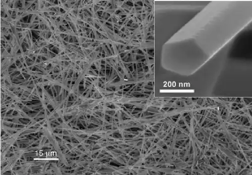
Nanowires (Si silicon/germanium Gi) , thin structures that are just a few billionths of a meter in diameter but thousands or millions of times longer, exist in a variety of forms—made of metals, semiconductors, insulators, and organic compounds—and are used in electronics, energy conversion, optics, and chemical sensing. Because they are so thin, nanowires with the (Si silicon/germanium Gi) structure are essentially one-dimensional. Nanowires are quasi-one-dimensional materials, “their two dimensions are on the nanometer scale.” This one-dimensionality confers distinct electrical and optical properties. For one thing, this means that electrons and photons in these nanowires experience “quantum confinement effects.” However, unlike other materials that produce such quantum effects, such as quantum dots, the length of nanowires allows them to communicate with other macroscopic devices and the outside world.
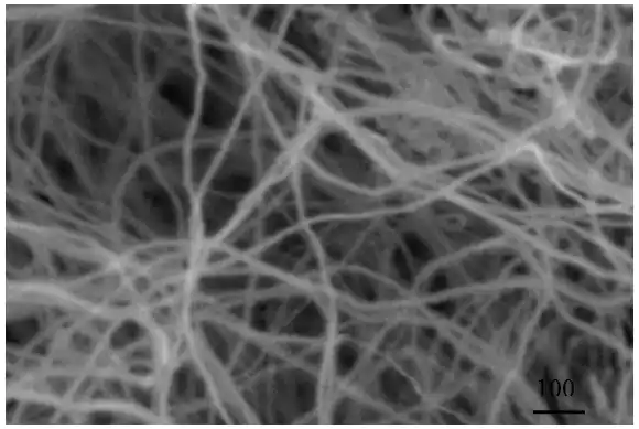
The structure of a nanowire is so simple that there is no room for defects, and electrons pass through unhindered. This is a big problem with conventional crystalline semiconductors, such as those made from silicon wafers: These defects are always present in those structures, and those defects interfere with the passage of electrons. In addition, materials that normally do not mix easily can be assembled into nanowires. For example, layers of silicon and germanium, two widely used semiconductors, “are very difficult to grow together in thin films.” “But in nanowires, they can be grown without any problems.” Moreover, the equipment required for this type of vapor deposition is widely used in the semiconductor industry and can be easily adapted to produce nanowires.
Conclusion :
Tiny filaments and cylinders of structured nanowires (silicon/germanium) are used for possible applications in energy, electronics, optics, and other fields.
Morphology and Phases of Nanowires/Nanotubes by Transmission Electron Microscopy (TEM) and X-ray Diffraction (XRD), Respectively
Investigation of a Focused Nano-Plasmonic Diaphragm Method With Nano-Electric Field Distribution in an Entangled Diaphragm Structure in an Aluminum Film at a Wavelength of Less Than ۲ nm