افشین رشید
اُستادیار ؛ عضو هیات علمی دانشگاه آزاد اسلامی واحد علوم و تحقیقات تهران
654 یادداشت منتشر شدهReview (Link Between Nanoelectronics and Nanoplasmonics) and Many Advantages Such as Ease of Production, Possibility of industrialization, Ability to Control The Dimensions of Raw Materials of Nanochips and Nanotransistors
Note: Among the common methods for producing nanostructures, stretching, molding, phase separation, self-assembly, and electrospinning, electrospinning has many advantages such as ease of production, the possibility of industrialization, the ability to control the dimensions of the raw materials of nanochips and nanotransistors, and repeatability.
The material that makes up most chips and nanochips is silicon. By applying an appropriate voltage (threshold voltage) to the silicon solution, the repulsive force overcomes the surface tension of the silicon and a jet is formed. As the solvent evaporates from the jet, the liquid phase changes to solid and the nanomaterials of the chips are formed. Many parameters affect the characteristics of the nanostructures produced by this method, the most important influential parameters are the distance between the needle and the collector, the applied voltage, the flow rate and the concentration of the silicon solution; by changing these parameters, the optimal dimensions of the nanochips can be achieved. The diameter of the nanostructures is linearly related to the flow rate and distance, and nonlinearly related to the potential and concentration of the silicon solution in the production of nanochips and nanotransistors. With increasing distance and electric potential, the diameter of the nanostructures decreases and with increasing current rate and electric potential, it increases. In the production of nanochips and nanotransistor molds, when the repulsive force overcomes the surface tension, the electric field reaches a critical or threshold value. Initially, the jet moves in a linear pattern, then slowly deviates from the linear pattern, forming a complex shape along the path towards the collector. The structure and construction of nanochips and nanotransistors and the length of the jet are proportional to the applied voltage. The structure of the Taylor nanocone changes from convex to concave with changing field strength and subsequently (jet charge density).
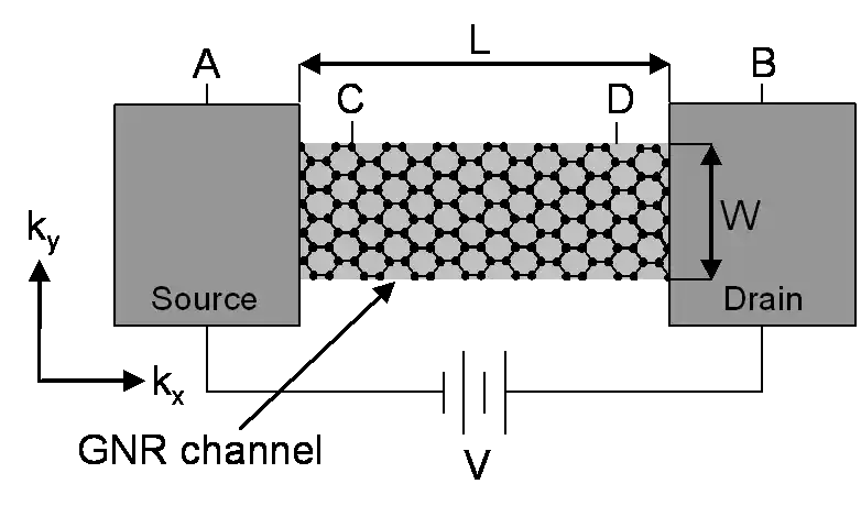
Note: The nanotransistor is one of the most important nano-electrical components that has functions such as circuit amplification, power supply, etc. and is used in the internal structure and construction of chips and nano-chips.
The miniaturization of components in microelectronic systems and circuits has led to significant growth in this industry in recent years. The growth rate of this industry is so high that as components become smaller, the number of transistors per unit area of each semiconductor chip and nanochip has increased. The miniaturization of these components can reduce the consumption of raw materials and energy, reduce the cost of these components, and increase their speed and efficiency. Therefore, the construction and development of electronic devices with smaller dimensions and greater speed and efficiency has become increasingly important. The lithography method is one of the common methods for manufacturing electronic circuits. With the help of this method, structures with precision and dimensions of 0.1 nanometers can be manufactured. Finding techniques that can be used to use this method for the industrial production of these components (nanochips and microchips).
Conclusion:
Among the common methods for producing nanostructures, stretching, molding, phase separation, self-assembly, and electrospinning, electrospinning has many advantages such as ease of production, the possibility of industrialization, the ability to control the dimensions of the raw materials of nanochips and nanotransistors, and repeatability.
Nano Gas Laser ( including Carbon Dioxide, Carbon Monoxide, Helium-Neon, Helium-Cadmium, Argon, Gripton, Nitrogen Molecules, Excimer, Copper Vapor, and Gold Vapor Nanolasers )
The RISC architecture and structure in CMOS memory derives its ability to perform from the "instruction set architecture" in which it is designed