افشین رشید
اُستادیار ؛ عضو هیات علمی دانشگاه آزاد اسلامی واحد علوم و تحقیقات تهران
654 یادداشت منتشر شدهElectron Beam Nanolithography Allows for Precise Control of Nanostructure Properties, Which is The Basis for Various Technologies in Nanoelectronics.
Note: Electron beam lithography enables precise control of nanostructure properties that form the basis of various nanotechnologies. The Nanostructure Fabrication and Measurement Group advances the precision of lithography at the nanometer scale, creating processes for the fabrication of innovative devices and standards in physical fields ranging from photonics to fluids.
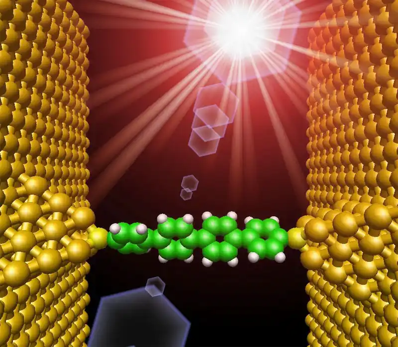
Electron beam nanolithography enables precise control of nanostructure features that form the basis of various device technologies. Lateral resolutions of 10 nm, placement accuracy of 1 nm, and patterning fields of 1 mm are all possible. However, achieving these performance metrics is dependent on interdependent factors that are specific to the sample—pattern definition and breakdown, substrate and mask materials, pre-exposure and post-exposure processes, alignment feature definition—as well as, importantly, the details of lithography system operation. As a core capability, and developing processes that are within or close to the limits of conventional electron beam lithography to advance nanoscale devices and measurement science in various fields, such as: chip-scale frequency combs for precise timekeeping; integrated nonlinear optics for wavelength and quantum frequency conversion; and cavity-based optomechanical and micro/nanoelectromechanical systems for nonlinear sensing, transport, and dynamics studies; Quantum photonic integrated circuits with nonlinear and quantum light sources for quantum information. Ultraviolet to infrared levels for trapping and probing atoms and ions, polarimetry, imaging and spatiotemporal ultrafast laser pulse shaping. Optical microscope standards for aberration correction and to advance fundamental capabilities in electron beam lithography, and developing methods to better control, measure and understand fabrication processes. To lower the barrier to entry of electron beam lithography and improve pattern precision control, the nanolithography toolbox is also applied. To improve pattern placement, electron beam lithography is used for pattern standards for atomic force correlation microscopy and super-resolution optical microscopy, with precise localization with high throughput and characterization and optimization of process parameters. Such measurements create a positive feedback loop for the fabrication and measurement of nanostructures.
The ability to fabricate large-scale micro- and nanostructures on non-planar surfaces is important for many applications such as optics, optoelectronics, nanophotonics, imaging technology, NEMS, and microfluidics. However, it is very difficult to fabricate large-scale nanostructures on curved or non-planar surfaces using existing patterning methods. In addition, a variety of current nanopatterning technologies, such as electron beam lithography, optical lithography, interference lithography (IL), etc., cannot cope with all the practical demands of industrial applications in terms of high resolution, high throughput, low cost, large area, and patterns on non-planar and curved surfaces. Therefore, new high-volume nanofabrication technology is in urgent need of exploitation and development to meet the extraordinary needs of growing markets. Nanoelectronic lithography is currently considered as a promising nanopatterning method with low cost, high throughput and high resolution, especially for the production of large-scale micro/nanoscale patterns and complex three-dimensional structures as well as high aspect ratio features . Due to these outstanding advantages, the transformation of optical structures in combination with large-scale fabrication becomes a more effective method in this field.
Conclusion :
Electron beam lithography enables precise control of nanostructure properties that form the basis of various nanotechnologies. The Nanostructure Fabrication and Measurement Group advances the precision of lithography at the nanometer scale, creating processes for the fabrication of innovative devices and standards in physical fields ranging from photonics to fluids.