افشین رشید
اُستادیار ؛ عضو هیات علمی دانشگاه آزاد اسلامی واحد علوم و تحقیقات تهران
651 یادداشت منتشر شده(Nanotransistor) and The Unique Properties of Graphene Such as High Electronic Mobility and Thermal Conductivity, Resistance to Fracture
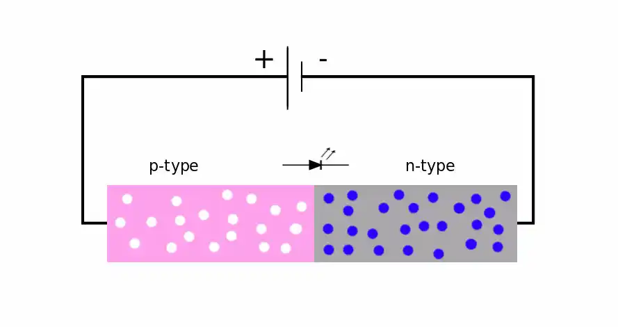
Note: The role of graphene nanosheets (GA) in the construction of a nanotransistor is that the electric field created by the gate electrode controls the current created by the two source and drain electrodes. The drain current transfer is modulated by changing the density of charge carriers in the two-dimensional transfer channel.
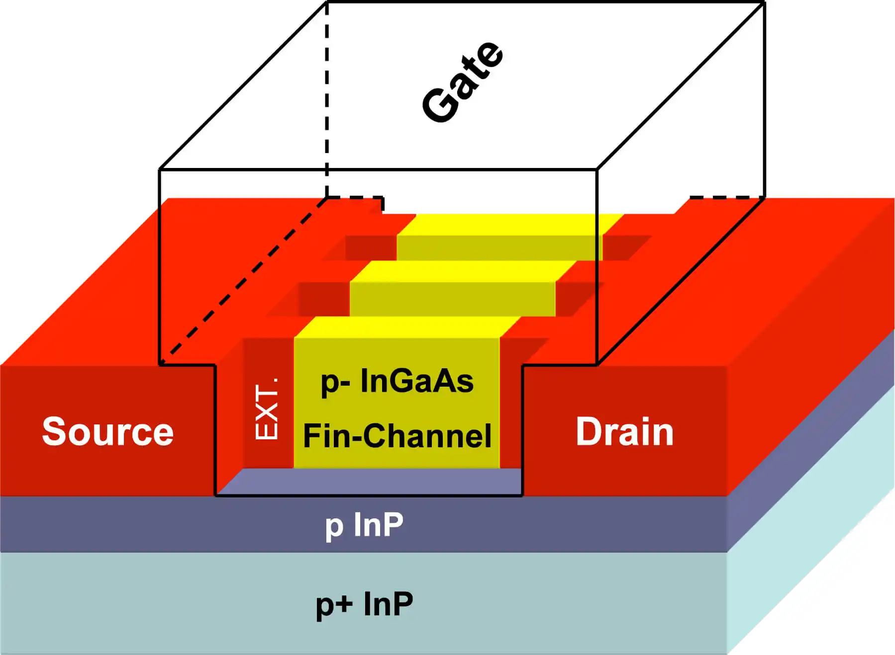
In the multilayer Si graphene field effect nanotransistor, a 3D conduction channel with a drain current modulated by the thickness of the 3D conduction channel . In the circuit diagram of a multilayer GA graphene field effect nanotransistor, the two source and drain electrodes are directly connected to the semiconductor, while the gate electrode is capacitively connected to the semiconductor using a gate dielectric. The design, manufacture, development and use of products whose size is in the range of 1 nmto nm is called nanoelectronics. In fact, we are talking about miniaturization, which enables more contact, more activity and increased area. Nano is a new scale in technologies and a new approach in all disciplines, and it gives humanity the ability to expand its intervention in the structure of materials and to design and manufacture at very small dimensions and to influence all the technologies that humanity has achieved so far.
Numerous chemical and physical methods have been proposed to produce different types of multilayer nanographene. The basic idea of physical methods is that in these methods, they try to eliminate the forces between the graphene sheets in graphite and separate them to obtain single layers of graphene or graphene oxide, which is the top-down method. In chemical methods, multilayer nanographene is made by placing individual carbon atoms together, which is also called the bottom-up method.
Conclusion:
The role of graphene nanosheets (GA) in the fabrication of nanotransistors is that the electric field generated by the gate electrode controls the current generated by the two source and drain electrodes. The drain current transfer is modulated by changing the density of charge carriers in the two-dimensional transfer channel.