افشین رشید
اُستادیار ؛ عضو هیات علمی دانشگاه آزاد اسلامی واحد علوم و تحقیقات تهران
651 یادداشت منتشر شدهIn field effect nanotransistors (back-gate and hybrid) , the silicon substrate acts as the gate, which in this structure is called the back gate
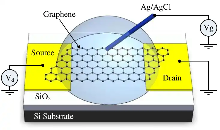
Note: In field effect nanotransistors (back-gate and hybrid) , the silicon substrate acts as the gate, which in this structure is called the back gate. Then, the top-gate nanotransistors , which were also suitable for use in integrated circuits similar to carbon nanotube-based transistorswith the addition of an upper gate separated from the nanotube channel by a thin oxide layer
The difference is that graphene is used in its channel instead of carbon nanotubes . Graphene's unique properties, such as high electron mobility and thermal conductivity, resistance to fracture, and low light absorption and band gap , make it possible to build high-speed electronic components in flexible and transparent electronic circuits using this nanomaterial.
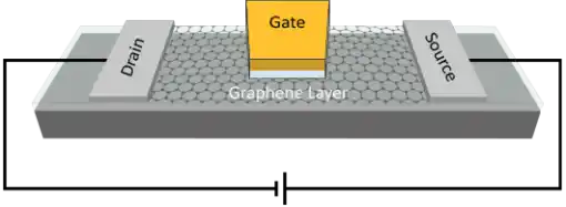
Common gate graphene nanotransistors can also have back and combination gate types (top and bottom) in terms of structure . Combination gates (Not; or; And; Nand) are used in the manufacture of nanochips using nanotransistors. The design , manufacture, development and use of field effect nanotransistors (back and combination gate) whose size is in the range of 1 nm to 100 nm is called field effect nanotransistor design . In fact, we are talking about miniaturization, which enables more contact, more activity and increased area. Nano is a new scale in technologies and a new approach in all disciplines and gives mankind the ability to expand its intervention in the structure of materials and to design and manufacture at very small dimensions and to influence all the technologies that mankind has currently achieved . And field effect nanotransistors (back and combination gate) (combined) has been considered in the production of electronic and biological nanotechnology. Implantable nanochips in the body and military industries depend on advances in the field of nanofield effect transistors (back-gate and hybrid) . Field effect nanotransistors ( back-gate and hybrid) are the main electronic components that are used as amplifiers in analog nanocircuits or electronic nanoswitches in digital circuits. And their advancement is the main key to nanoelectronics in the field of production and monopoly (nanochips) both in the field of military and biological industries. Field effect nanotransistors (back-gate and hybrid) and the technology for manufacturing integrated nanocircuits have become the most common based on them, namely CMOS technology in the micro and nanoelectronics industry. This industry and technology for manufacturing integrated circuits, this advantage of nanoelectronics in reducing the size of transistors and the number of transistors used in each chip, doubles. The shrinking of transistor dimensions leads to increased speed and reduced power losses. Nanotube-based field effect transistors and carbon-based field effect transistors, nanofield effect transistors (back-gate and hybrid) are very serious candidates to replace graphene and conventional silicon transistors.
Conclusion:
In nanofield effect transistors (back-gate and hybrid) , the silicon substrate acts as the gate, which in this structure is called the back-gate. Then there are top-gate nanotransistors , which were also suitable for use in integrated circuits , with the addition of a top gate separated from the nanotube channel by a thin oxide layer. Nanofield effect transistors are similar to carbon nanotube-based transistors.