افشین رشید
اُستادیار ؛ عضو هیات علمی دانشگاه آزاد اسلامی واحد علوم و تحقیقات تهران
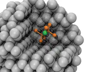
651 یادداشت منتشر شدهNano-assemblers can include Nano-transistors and Nano-diodes or Even Parts of Nano-Robots

Note: These devices, which include nanotransistors and nanodiodes, can be used in nanometer robots, nanoelectromechanical systems (NEMS), microelectromechanical systems (MEMS), and microfluidic devices. The mechanical action required to initiate deformation can be the pressing of a key, the pressure caused by the passage of a fluid, the stretching of muscles, or the movement of a robot's limbs.
Nano-microelectronics deals with new methods for making nano-transistors on a small scale , the dimensions of which are several tens of nanometers, which is derived from the science called nanotechnology. Unlike today's nanotransistors, which behave based on the movement of a mass of electrons in matter, the new devices follow quantum mechanical phenomena at the nano scale, in which the discrete nature of electrons cannot be ignored. By reducing all the horizontal and vertical dimensions of the transistor, the electric charge density in different areas of the nano-transistor increases, or in other words, the number of electric charges per unit area of the nano-transistor increases. This event has two negative consequences : First, with the increase in electric charge density, the possibility of electric charge discharge from the insulating areas of the transistor increases , and this event causes damage to the transistor and its failure. This event is similar to the discharge of excess electric charge between the cloud and the ground in the phenomenon of lightning, which causes the ionization of air molecules into negative and positive ions. Secondly, with the increase of the electric charge density, the electrons may leave the range of the radius of one atom and enter the range of the neighboring atom's radius under the influence of repulsive or abduction forces whose value has now increased. This is called tunneling in quantum physics. Electron tunneling from one atom to the adjacent atom is a phenomenon that happens a lot between electrons in small dimensions. This phenomenon is the basis of some electronic components and some nanoscopes. But in nanotransistor, this phenomenon is not a useful phenomenon, because electron tunneling from one atom to the adjacent atom may continue and cause an electric current. Although this electric current may be very small, but because it is unwanted and unanticipated, it acts as a leakage path for electric current and changes the electrical behavior of the nano-transistor.
One of the industries that benefit the most from the growth of nanotechnology is the electronics industry. Computers and their parts are designed in such a way that they are constantly moving towards reducing and optimizing the dimensions of the parts. In such a situation, the role of nanotechnology in the computer can turn the eyes towards itself. Nanotechnology is the field of application of extremely small components next to each other. In the case of computers, the goal of putting these nanometer components together is to build faster, more powerful and smoother functioning computers in a smaller volume. which are used in nano-micro electronic systems. Nano technology has played a major role in the design scenario of newer and faster computers.

Conclusion:
These devices, which include nanotransistors and nanodiodes, can be used in nanometer robots, nanoelectromechanical systems (NEMS), microelectromechanical systems (MEMS), and microfluidic devices. The mechanical action required to initiate deformation can be the pressing of a key, the pressure caused by the passage of a fluid, the stretching of muscles, or the movement of a robot's limbs.