افشین رشید
اُستادیار ؛ عضو هیات علمی دانشگاه آزاد اسلامی واحد علوم و تحقیقات تهران
651 یادداشت منتشر شدهApplication of graphene in nano materials for electrostatic discharge and shielding of interference nano-electromagnetic waves
Note: The use of graphene nano strips in the characteristics of nano electrostatic discharge materials (Nano ESD) is the surface resistance between 1012 and 105 Ω. While nano-electromagnetic interference protective materials (Nano_EMI) must have a resistance of less than 105 Ω.
The application of graphene nano-ribbons in nano-interference electromagnetic shielding materials and nano-electrostatic discharge in nano-electronic devices has expanded to Rectenna nano-antennas and nano-supercapacitors. The efficiency of graphene particles in electromagnetic interference shielding and enhanced with modified graphene nanoribbons is measured. One of the important and new structures of carbon nanostructures is graphene. Graphene is a sheet of carbon atoms that forms a hexagonal dovecot structure with 2Sp and SP3 bonds . There are single-layer, double-layer and multi-layer graphenes . With its low thickness, this material is the hardest known material. Graphene is very transparent because it has a thickness of one atom and allows light to pass through it and has high nano electrical conductivity.

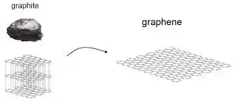
Graphene is the newest member of the large carbon family. The term graphene was used to describe a single nano layer of graphite. This nano material has high transparency due to its small thickness. Also, its conductivity has caused it to attract a lot of attention. It is very difficult to control the conditions to separate a single layer of graphene, usually the prepared material called graphene consists of a set of several layers of graphene, each of which contains a different number of sheets. Graphene does not exist with a completely flat atomic structure, graphene sheets are flexible, that is, they bend, fold, or their surface becomes wavy. The large bends are related to the method of preparing graphene, and the small waves are the inherent properties of separated layers .
Conclusion :
This new semiconductor (graphene) has been used in electrostatic discharge nanomaterials and electromagnetic interference nano wave protection. Normally, this material is used in making high-speed transistors and lasers. This material can be easily produced and used, and from now on, it can be of high value in terms of nanostructure and physical properties, and in the manufacture of electronic devices, especially in the manufacture of nanodevices at the industrial level.