افشین رشید
اُستادیار ؛ عضو هیات علمی دانشگاه آزاد اسلامی واحد علوم و تحقیقات تهران
654 یادداشت منتشر شدهnMOS Transistors (Correct Pronunciation: en _ mos) Amplify The Current Depending On The Direction of The Electric Field
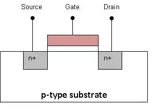
Note: In nMOS transistors, current amplification varies depending on the direction of the electric field and responds to electric fields of different sizes. This results in useful electronic behavior depending on how the voltage (or electronic field ) is applied, which in an nMOS transistor is called (bias).
nMOS transistors use a voltage to apply to the input terminal, which is called the gate, and the current passing through it is proportional to this voltage.
Since the operation of nMOS transistors is based on an electric field resulting from the input gate voltage (the name field effect is for this reason), it makes the field effect transistor a voltage-based component. nMOS transistors are a single-pole semiconductor device whose characteristics are very similar to the same bipolar transistor. Some of the features of this part are high efficiency, instantaneous operation, resistance and cheapness, which can be replaced in most electronic circuits with bipolar junction transistors and structurally similar (such as BJT).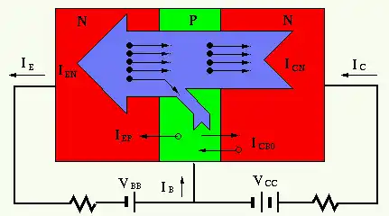
Understanding how an nMOS transistor works is difficult because it involves fairly advanced quantum mechanics. However, at the simplest level, the operation of an nMOS transistor can be understood by looking at the flow of positive charges (or "holes ") and negative charges (electrons). pn junctions are also important in the operation of a transistor. Proper operation of the nMOS transistor requires a process known as biasing . Semiconductors can be left with materials so that they are more than electrons that are easily displaced - which is generally used in the negative or n-type region . In general, as a hint - also, they can be made with elements that create an over-hole that easily absorbs these doped electrons or p -type region.
The transistor must be biased for two reasons:
The transistor must work in the active region. The value of the small signal parameters (ro, gm) depends on the amount of dc current passing through the transistor. We always perform a DC analysis first, so that the operating point of the transistor can be determined and we can calculate the parameters of the small signal. Then we zero the DC sources and start the AC analysis using the small signal model . One of the important characteristics of transistor bias in the above circuit is that the potential (collector) is always higher than (base), so the transistor will always be in the active region.