افشین رشید
اُستادیار ؛ عضو هیات علمی دانشگاه آزاد اسلامی واحد علوم و تحقیقات تهران
654 یادداشت منتشر شده(Nanoelectronics) Principles of Manufacturing and Classification of MEMS
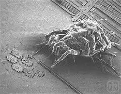
Note: MEMS are used in systems that are classified by nanoelectronics for defense, pharmaceutical, medical, electronic, and telecommunication applications, etc. Current MEMS include accelerometers, projection display chips, drone sensors, optical switches, microvalves, biosensors, and multipurpose microchips that are produced in nanoscale volumes.
MEMS are integrated into moving microstructures (with electromechanical components), sensors, actuators, radiative energy devices , and microelectronics. These MEMS can be fabricated for use in various microfabrication technologies such as micromachines . The fundamental technology in the fabrication of MEMS is CMOS and biCOMS (for the fabrication of ICs) and micromachines (for generating motion and radiating energy to micron-scale devices and structures ). One of the main goals is to integrate microelectronics with electromechanical micromachinery devices and structures to produce integrated, high-performance MEMS . To ensure high performance, workability, reliability, and manufacturability, CMOS-based bulk fabrication processes are well developed and need to be refined and enhanced.
Micromachining (bulk and bulk ) (as well as LIGA-like and LIGA-like) are the most developed fabrication methods. Silicon is the primary substrate material used in the microelectronics industry. A crystal mold (a solid cylinder 300mm in diameter and 100mm in length) of very high purity silicon is crystallized, cut to the desired thickness, and then polished using mechanical and chemical polishing technologies . The properties of the electromagnetic and mechanical plates are the direction and location of crystal crystallization and its expected impurities.
Depending on the silicon substrate, CMOS and biCMOS processes are used to manufacture ICs and the processes are classified as: n-well, p -well or twin-well. The main steps are: diffusion, oxidation , polysilicon gate formation, photolithography, gate formations, masking, etching, metallization, wire bonding, etc.