افشین رشید
اُستادیار ؛ عضو هیات علمی دانشگاه آزاد اسلامی واحد علوم و تحقیقات تهران
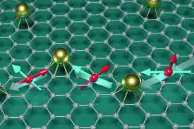
651 یادداشت منتشر شدهFabrication of Nanoelectronic Circuits in the Development and Reduction of The Volume of Smart Electronic Circuits
Note: With the advent of emerging nano-microelectronics technology, the precision of device manufacturing machines has not improved in line with the shrinking dimensions of transistors.
This effect, together with the reduction of power supply voltage and transistor threshold voltage, has caused a sharp decrease in the efficiency of device fabrication in nanotechnology. Traditional methods of modeling and compensating for the effects of inter-chip and intra-chip variations, such as modeling in the worst-case corners, are no longer applicable, and the need for accurate statistical methods to increase design efficiency is strongly felt.

To reduce the area of integrated circuits, SRAM memory arrays are usually fabricated with the smallest possible channel length and width, which increases the destructive effects of process variations. After examining the various failure mechanisms in nanotechnology memory cells (read, write, hold errors, etc.), a method for optimizing the efficiency of FinFET-based memory cells is presented.

This method exploits the dynamic power-variability of the FinFET transistor by modulating its back-channel voltage. As transistor dimensions are reduced in nanoscale technologies, traditional methods for timing analysis of combinational circuits lose their efficiency.
The main technique in the manufacture of electronic circuits is the use of optical lithography. In fact, the reason for the rapid growth of the electronics industry was this simple but very widely used method, which makes it possible to manufacture an infinite number of transistors in a short time.
To reduce the size of transistors, it was necessary to prepare smaller masks so that various parts of electronic circuits could be made on a silicon wafer by shining light beams on these masks. Although making smaller masks using electron beams was very expensive, it seemed possible;
The main challenge was the behavior of light rays at small scales. In fact, light rays at small scales behave differently than at large scales, making it difficult to build nanoscale circuits.