افشین رشید
اُستادیار ؛ عضو هیات علمی دانشگاه آزاد اسلامی واحد علوم و تحقیقات تهران
615 یادداشت منتشر شدهFinFET nanotransistor downscaling causes more short channel effects, less gate control, exponential increase in leakage currents, drastic process changes and unmanageable power densities

Note: Since the FinFEET nanotransistors in to achieve, a larger discharge current in the nanotransistor, the width of the channel according to the height as well as the thickness, which the layers of nano CNTs It keeps it in a smaller range.
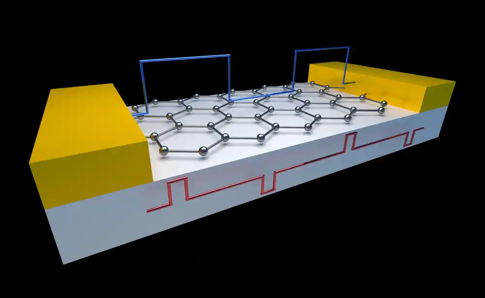
FinFEET nanotransistors are a field-effect nanotransistor metal-oxide-semiconductor ) that is on a substrate < a i=3> is made. that the gate is located on two, three or four sides of the channel or is wrapped. The channel forms a double gate structure. To these devices, the general name "finfets" given because the source/drain region forms fins on the silicon surface. FinFET devices compared to flat technology and using nanowires in the structure and (complementary metal oxide and semiconductor) < a i=8>have significantly faster switching and higher current density.
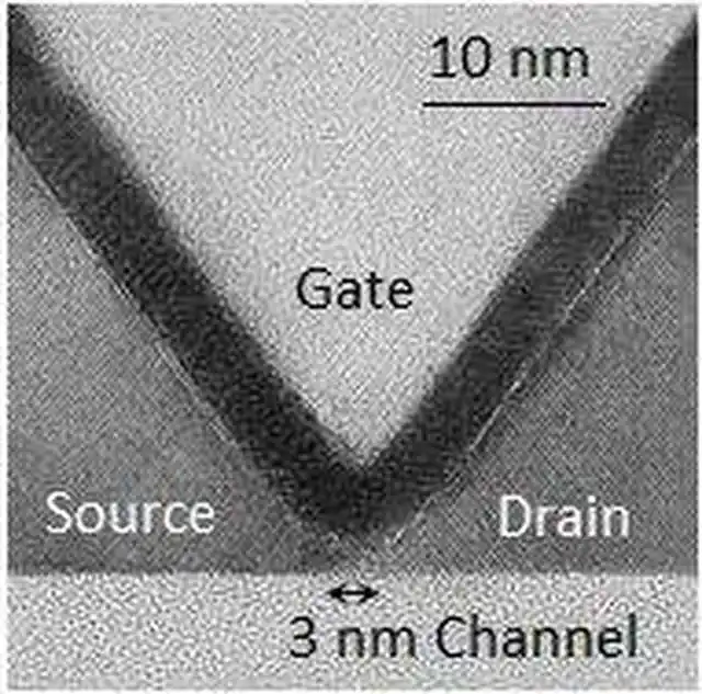
Due to the reduction of the scale of semiconductor components and integrated circuits to the nanometer range, in the FinFET nanotransistor, the reduction of scale causes more short channel effects, less gate control, an exponential increase in leakage currents, severe process changes and power densities. It becomes unmanageable. The connection between the carbon and metal nanotubes used to connect the source and the drain forms the Schottky barrier (SB) in a FinFET nanotransistor. The formation of Schottky barriers in the source and drain of a transistor causes a significant decrease in the drain current of FinFET nanotransistors. Therefore, for the higher operational efficiency of Finfet nanotransistors parts, suitable metals are needed that can be used in the source and drain junctions of the nanotransistor and create an ohmic connection. The ability of carbon nanotubes to be used in FinFET nanotransistors is hollow and high Being their contact surface. This contact surface consists of the outer wall of the nanotube and its empty middle parts. In FinFET nanotransistors, when an electric field is applied , the carbon nanotube located between the source and drain contains the moving charge. It becomes. The density of these charges is 5 for the source and this density is determined by the electric conduction in the multi-layered nanotubes for 6 there is also a possibility of Fermi-Dirac distribution. a
Conclusion :
Since FinFEET nanotransistors in to reach, a larger discharge current in the nanotransistor, the width of the channel according to the height as well as the thickness, which the layers of nano CNTs It keeps in a smaller range.