افشین رشید
اُستادیار ؛ عضو هیات علمی دانشگاه آزاد اسلامی واحد علوم و تحقیقات تهران
651 یادداشت منتشر شدهPlanar FET" nanotransistors"
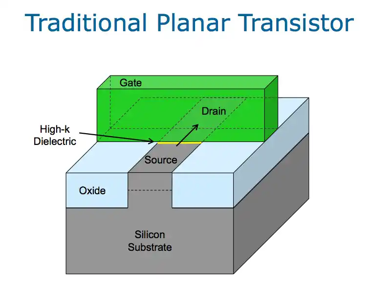
Note: Planar FET nanotransistors are a planar structure, which basically consists of three components: gate, collector and base or gate, which controls the flow of electrons between the two by means of nanowires.
Planar FET nanotransistors In a thin nano layer under the gate, called the inversion layer, is responsible for the entire flow of electrons, and a tiny nano wire between the two poles of an electrical outlet behaves This wasn't a problem when transistors measured 180 nm or so, but as they got smaller, the inverted nanolayer got thinner and thinner and became less efficient. As a result, even when the transistor is off (gate leakage), more energy and current flows between the emitter and collector, and the voltage difference between the two states is smaller.

By reducing gate leakage through technologies such as nanowires, Nano wire causes a simple voltage to pass through the gate, which forces more electrons to pass through the inversion nanolayer. It reduces the voltage drop problem in planar FET nanotransistors, resulting in a much larger contact area and better control of electron flow. Since there are now three points to be placed between the nanolayer inversion layer and the contact gate of the Planar FET nanotransistors, the transistors based on the nanoPlanar FET technology, even if the logic performance is the same, with a The single gateway makes contact at three points.
Conclusion :
Planar FET nanotransistors are planar structures, consisting of basically three components: emitter, collector, and base or gate, which controls the flow of electrons between the two by means of nanowires.