افشین رشید
اُستادیار ؛ عضو هیات علمی دانشگاه آزاد اسلامی واحد علوم و تحقیقات تهران
654 یادداشت منتشر شدهtransistor nMOS (with ultra-low power consumption, energy-efficient computing, during the sub-threshold range)

Note: field effect tunnel transistor nMOS is an experimental type of transistor. Even if its structure is very similar to a metal-oxide semiconductor field effect transistor nMOS , the basic switching mechanism in These two transistors differ from each other, nMOS instead of thyrmonic emission modulation. 8> on a barrier, such as traditional nMOSs, with quantum tunnel modulation 12> They change through a dam.
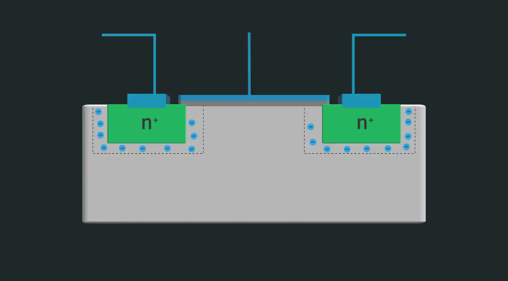
field-effect tunneling transistor nMOS, as an alternative to conventional CMOS by enabling the voltage supply (VDD) with power consumption Ultra-low, energy-efficient computing occurred during the sub-threshold slope (SS) range. That type of device is a reverse-bias gate structure, which is usually called a tunnel field-effect transistor nMOS . For low power applications, nMOS is considered. This device has less static leakage current than MOSFET and is more resistant to SCEs.
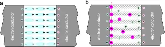
The most outstanding feature of nMOS s is the capacity to produce a reverse subthreshold swing (SS) of less than 60 mV/decade thermal limit (at 300 K ) is related to common reverse mode nMOSs. Pseudo-thermal ss is achievable because the drain current in nMOSs is generated by source-to-channel carrier injection, which is often under the band tunneling radius. It is placed in the quantum mechanical band (BTBT).
transistor speed nMOS is proportional to the current. The higher the current, the faster the transistor will be able to amplify and charge (sequential capacitor voltage). For a given transistor speed and maximum acceptable subthreshold leakage, the subthreshold slope thus defines a minimum threshold voltage. Decreasing the threshold voltage is an essential part of the idea to scale the constant amount of nMOS .to overcome some challenges associated with the nMOS structure, such as its need for ultra-sharp doping profiles; However, such devices may suffer from gate leakage due to the presence of large vertical fields in the nMOS transistor structure. .