افشین رشید
اُستادیار ؛ عضو هیات علمی دانشگاه آزاد اسلامی واحد علوم و تحقیقات تهران
654 یادداشت منتشر شدهNanolithography techniques (optical and electron beam) periodic up to ۵۰ nanometers

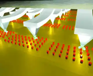
Note: Nanolithography techniques (optical and electron beam) periodically up to 50 nanometers Able to directly remove materials without much use It is one of the resistances. As a direct nanolithography method, the number of processing steps is minimized compared to other methods.
Nanolithography techniques (optical and electron beam) periodic up to 50 nm As a sequential nanolithography technique, it is inherently slow and its throughput is much lower than Various techniques and Liquid metal ion source based on nano-tools to the most extensive type of source in Nanolithography equipment (radiation optical and electronic) periodic up to 50 nm has been converted. However, in recent years, new developments in sources such as gas field ion sources, plasma sources and Metal alloy sources are the next step in terms of clarity or power.

Since the ion-matter interaction is stronger than the electron-matter interaction, it is possible to create harmful effects on the remaining material and change its physical and chemical properties. Important but key applications for nanolithography (light and electron beam) technology have been found in the semiconductor industry, in nanotechnology, and in materials science. and deposition caused by nanolithography (optical and electron beam) requires a gas injection system to replace a material The device, which is delivered in gaseous form, produces a local deposition by dissociating the precursor created by appropriate radiation in nanoelectrical devices. The main advantage of this technique is the selective growth of a material in the region of interest in one step. Due to the high resolution of the technique Nanolithography (optical and electron beam) , deposits can be made with high lateral resolution Gad , but due to much less damage caused to the substrate due to the lower linear motion of electrons compared to ions. On the contrary, the growth rate and metal content in deposits in general for nanolithography (optical and electron beam) to has come into being.
Conclusion :
Nano lithography techniques (optical and electron beam) up to the range of 50 nanometers are able to remove materials directly without using a lot of resistors. As a direct nanolithography method, the number of processing steps is minimized compared to other methods.