افشین رشید
اُستادیار ؛ عضو هیات علمی دانشگاه آزاد اسلامی واحد علوم و تحقیقات تهران
654 یادداشت منتشر شدهNano-Transistor (GAAFET) Approaches ۵nm
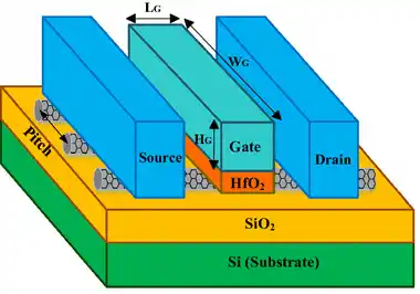
Note: As the fin width in a nano-transistor (GAAFET) approaches 5nm, variations in the width of the surrounding gate field-effect nano-transistor channel can cause undesirable changes and loss of mobility.
A nanogate transistor—the gate around the FET—can get around the problem. And electrostatically, an all-gate gate is a nanotransistor in which a gate is placed on all four sides of the channel. It’s essentially a silicon nanowire with a gate wrapped around it. In some cases, the surrounding FET can have a common gate or other material in the channels. Horizontal layered nanovolts are emerging as the consensus for 5-nanometer transistors. These devices start with alternating layers of silicon and silicon germanium (SiGe) that are patterned into columns. Creating the initial Si/SiGe heterostructure is straightforward, and the columnar pattern is similar to the fin structure for the nanotransistor. For some GAAFET nanosheet transistors, the indentation in the SiGe layers creates an internal gap between the source/drain, which ultimately lines up with the column and the space where the nanotransistor’s gate is located. This gap determines the gate width. Then, once the internal gaps are in place, an etch removes the free SiGe channel. The gate dielectric nanolayer and metal are placed in the spaces between the silicon nanowires. To minimize lattice distortion and other defects, the germanium content of the SiGe layers should be as low as possible. The selectivity of the nanolayer in the surrounding gate nanotransistor increases with the Ge or germanium content, and the erosion of the silicon layers during the indentation of the internal gaps or gate-channel release of the nanotransistor and the channel affects the thickness of the surrounding gate channel and thus the threshold voltage.
The structure of Gate-Around Field-Effect Nanotransistors (GAAFET) using (Carbon Nanotube) represents a new class of semiconductor materials consisting of a single sheet of carbon atoms stacked to form a tubular structure. GAAFET is a field-effect transistor (FET) that uses the semiconductor CNT as a channel material between two metal electrodes, which behave as source and drain contacts.
Conclusion :
As the fin width in a nano-gate field-effect transistor (GAAFET) approaches 5nm, variations in the width of the surrounding gate field-effect nano-gate transistor channel can cause undesirable changes and loss of mobility.