افشین رشید
اُستادیار ؛ عضو هیات علمی دانشگاه آزاد اسلامی واحد علوم و تحقیقات تهران
651 یادداشت منتشر شدهNano Transistors Acquire Magnetic Properties in Strong (Nanoelectromagnetic) Fields
Note: In the nanotransistor structure, the electronic quantity that is more easily accessible is the ionization potential, and in the nanostructure, the ionization potential is higher in the size of small grains (smaller particles), meaning that as the size of the particles increases, their ionization potential decreases.
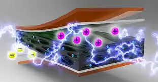
Increasing the surface area to volume ratio and changes in geometry and electronic structure have a strong impact on the chemical interactions of the material, for example, the activity of small particles changes with changes in the number of atoms (and therefore the size of the particles). Unlike today's nanotransistors, which behave based on the movement of a mass of electrons in the material, new devices follow quantum mechanical phenomena at the nanoscale, in which the discrete nature of the electron can no longer be ignored. By reducing all horizontal and vertical dimensions of the transistor, the electric charge density in various regions of the nanotransistor increases, or in other words, the number of electric charges per unit area of the nanotransistor increases.

This has two negative consequences:
First, as the electric charge density increases, the possibility of electric charge discharge from the insulating areas of the transistor increases, and this causes damage to the transistor and its failure. This is similar to the discharge of excess electric charge between the cloud and the ground in the phenomenon of lightning or thunder, which causes the ionization of air molecules into negative and positive ions. Second, as the electric charge density increases, electrons may, under the influence of repulsive or attractive forces, which have now increased in value, leave the radius of an atom and enter the radius of an adjacent atom. This phenomenon is called tunneling in quantum physics. The tunneling of electrons from one atom to an adjacent atom is a phenomenon that occurs frequently in small dimensions between electrons. This phenomenon is also the basis of the operation of some electronic components and some nanoscopes. However, in a nanotransistor, this phenomenon is not a useful phenomenon, because the tunneling of electrons from one atom to an adjacent atom may continue and cause an electric current. Although shrinking transistors and entering dimensions below 100 nanometers within the functional range of nanoelectronics technology has many advantages, it faces various challenges.
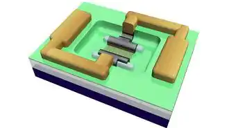
The design, manufacture, development and use of products whose size is in the range of 1 nm to 100 nm is called nanoelectronics. In fact, we are talking about miniaturization, which makes it possible to have more contact, more activity and increase the area. Nano is a new scale in technologies and a new approach in all disciplines, and it gives humanity the ability to expand its intervention in the structure of materials and to design and manufacture at very small dimensions and to affect all the technologies that humanity has achieved at present . And this trend has been taken into account in the production of nanotransistors Nano transistor .
Conclusion :
In the nanotransistor structure, the electronic quantity that is more easily accessible is the ionization potential, and in the nanostructure, the ionization potential is higher in the size of small grains (smaller particles), meaning that as the size of the particles increases, their ionization potential decreases.