افشین رشید
اُستادیار ؛ عضو هیات علمی دانشگاه آزاد اسلامی واحد علوم و تحقیقات تهران
651 یادداشت منتشر شدهClassical Application Methods of Nanolithography On a (Spin Substrate) in The Fabrication of Nanowires
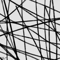
Note: Classical nanolithography application methods on a spin substrate are based on the specific interactions between these polymers and the substrate . Under certain conditions, the two types of polymers tend to form an interlocking pattern , there is a local order between both polymers, and they form nanowire-like domains with a period in the range of 50 nm.
This pattern would be very useful if subsequently applied to the classical nanolithography application which, after landing on the substrate, tends to accumulate on top of the polymer due to its lower diffusion mobility. Thus, the underlying thin structure follows the polymer scaffold, which extends without disturbance over several microns. However, the formed nanowires reveal some unwanted features as a closer look reveals significant roughness in the fabrication of the nanowires, as well as the nanowires being cut at certain points and deviating from the straight shape, all of which are typically the origin of the deterioration of the physical properties of the nanowires. Furthermore, the long-range ordering of the fabricated nanowire array following this strategy is not achieved, which is essential in certain applications such as the semiconductor industry.
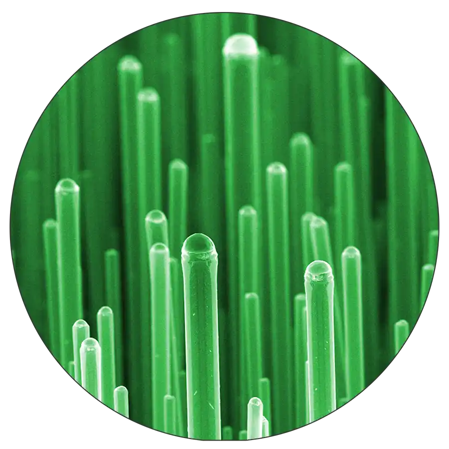
Nanowires are high aspect ratio and large area quasi-dielectric nanostructures, where the uniformity of radial strain allows for unusable combinations of semiconductor materials. It enables numerous applications of nanowires in electronics, optics and quantum technologies in general. In the propagation of nanowires particles are synthesized by counting nanowire particles embedded in an alumina template in air. The morphology and phases of nanowires/nanotubes are investigated by transmission electron microscopy (TEM) and X-ray diffraction (XRD), respectively. The electronic reaction of nanowire particles between oxidation plays a role in the formation of such nanowire nanostructures.These small nanowires are created by nanoparticle with diameters of nanometers. Nanotechnology is the study of materials at dimensions of approximately 1 to 100 nm, where only one of its kind phenomena offers descriptive applications. Nanotechnology encompasses science, engineering and technology that is not scaled down, imaging, measuring, designing and manipulating materials at this length scale. Due to nanotechnology, computers have become faster than ever before and the cost of calculations has decreased. Nanowires are made on a flat substrate of semiconductor materials such as silicon and germanium. Nanowires are very small wires. They are made of metals such as silver, gold or iron. A nanometer is a spatial measurement of about 10-9 meters, which is mostly used in nanotechnology to build nano machines. This small nanowire is created by nano particles with a diameter of nanometers.
Conclusion :
Classical application methods of nanolithography on a spin substrate Due to the specific interactions between these polymers and the substrate , under certain conditions, the two types of polymers tend to create an interwoven pattern , there is a local order between both polymers, and form nanowire-like domains with a period in the range of 50 nm.