افشین رشید
اُستادیار ؛ عضو هیات علمی دانشگاه آزاد اسلامی واحد علوم و تحقیقات تهران
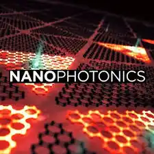
651 یادداشت منتشر شدهNano-Fullerenes and Their Application in Various Fields Such as Electronic Applications Such as (Fabrication of Nano-Electrodes Used in Specific Electrical Circuits, Nano-Photonics in Nano-Solar Cells, and Nano-absorbers of Specific Wavelengths)
Note: Fullerenes are identified by the number of atoms in their structure. Fullerenes are named using the letter C, which represents the number of carbon atoms in their structure.
Fullerenes are among the materials on which many nanomaterials are based. Their unique structural and electronic properties, as well as their use in various fields such as electronic applications such as the manufacture of nanoelectrodes used in specific electrical circuits, nanophotonics in nanosolar cells, and nanoabsorbers of specific wavelengths.

Nanotube layers can behave like a metal and be electrically conductive. Changing their structure and structure can make them exhibit semiconductor properties. Or they can be non-conductive. For example, a slight change in the helical section can transform the tube from a metal to a large-gap semiconductor.

Nanotube layers can behave like a metal and be electrically conductive. Changing their structure and structure can make them exhibit semiconductor properties. Or they can be non-conductive. For example, a slight change in the helical section can transform the tube from a metal to a large-gap semiconductor.
Conclusion :
An important feature of all nanostructures is that the number of surface atoms in them is greater than the number of bulk atoms. This ratio increases as the size of the nanoparticles decreases in fullerenes .