افشین رشید
اُستادیار ؛ عضو هیات علمی دانشگاه آزاد اسلامی واحد علوم و تحقیقات تهران
651 یادداشت منتشر شدهHigh speed (doping) nMOS graphene transistor in p- and n-doping electronic circuits (positive and negative)
Note: The term graphene nMOS transistor comes from the combination of the words graphene and nMOS transistor in transmission and resistance.
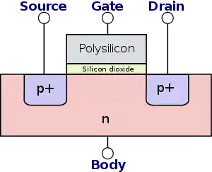
In a nMOS graphene field effect transistor, the resistance between two electrodes can be transferred or controlled by a third electrode. In a multilayer graphene field effect nMOS transistor, the current between the two electrodes is controlled by the electric field from the third electrode. Unlike the bipolar transistor, it is capacitively connected to the third electrode and is not in contact with the semiconductor. Three electrodes in the structure of the nMOS graphene field effect transistor are connected to the source, drain and gate, and this action increases the switching speed (doping) in the nMOS graphene transistor circuit.
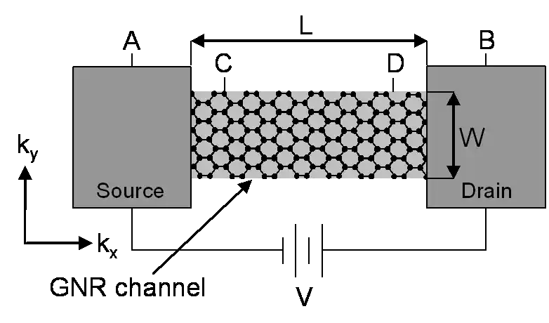
Graphene in nMOS field-effect transistors is an excellent electrical conductor, and also has outstanding spintronic properties. The ultra-thin carbon lattice is capable of transporting electrons with coordinated spin over longer distances and spinning for longer periods of time than any other known material at room temperature. Although the distance is still on the scale of a few micrometers and the time is still measured in nanoseconds, it essentially opens up the possibility of using rotation in microelectronic components.
The high speed of switching (doping) in the nMOS transistor circuit of Graphene transistor is possible only because it can do p- and n (positive and negative) doping, and graphene doping is a main parameter in the development of nMOS transistor Graphene transistor. The bias voltage is applied to the graphene transistors in such a way that it always operates in its "active" region, that is, the curved or active linear part is used for the output characteristics. Graphene, which consists of only one carbon atom, can be used to create multilayer graphene field-effect transistors that consume less energy and take up less space.Graphene is a semi-conducting material with zero gap and not suitable for logic circuits, but using technology, they create different forms of this material that have different gaps. Graphene strips, multilayer graphene and graphene grown on different transistor layers are such forms.