افشین رشید
اُستادیار ؛ عضو هیات علمی دانشگاه آزاد اسلامی واحد علوم و تحقیقات تهران
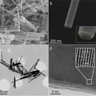
588 یادداشت منتشر شدهMorphology and Phases of Nanowires/Nanotubes by Transmission Electron Microscopy (TEM) and X-ray Diffraction (XRD), Respectively
Morphology and Phases of Nanowires/Nanotubes by Transmission Electron Microscopy (TEM) and X-ray Diffraction (XRD), Respectively
Note: Cobalt nanowire technology is at the material level, at approximately 1 to 100 nanometers in size, where only one of its kind phenomena offers descriptive applications.
Cobalt nanowires exhibit electromagnetically absorbing behavior at moderate temperatures, and when a magnetic field perpendicular to the direction of the nanowires is applied, these nanoelectronic devices have a larger coercive field than when a parallel electromagnetic field is applied to the cobalt nanowires. Nanotechnology encompasses science, engineering, and non-scale technology, including imaging, measuring, designing, and manipulating materials at this length scale. Due to nanotechnology, computer speeds have increased compared to the past and the cost of calculations has decreased. In the immersion method, the nanowires have enough time to transfer from the nanowire particles to the cavities; the formation stage of uniform nanoparticles is carried out slowly and finally uniform nanowires are formed. Structural investigation with FESEM in the immersion method, the nanowires are formed uniformly in all the pores and over a large area in the nanowire particles. The simple answer to this question is that each particle is less than 100 nm. But like the scale from 1 - 100 nm determines the size range of a nanoparticle. In order to avoid contact of cluster particles of atoms, it may be removed below 1 nm, but the electron movement in nanoparticles has to particles <1 nm. Since the particles are three-dimensional.
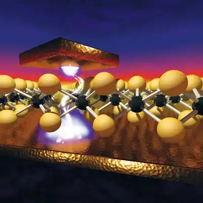
Cobalt nanowires with a diameter of about 93 nm are fabricated by electrospinning on an aluminum template. The nanowires are fabricated by galvanostatic deposition. The aluminum template is fabricated by multi-step monodization of pure aluminum foil. The fabrication of arrays of vertically aligned cobalt nanowires on flat surfaces and field emission (FE) using them as electron cathodes is achieved by electrodeposition in nanoparticle templates on Au/Ti/Si substrates at very low temperatures (<100 °C). After template removal, the arrays consist of structurally upright nanowires with high aspect ratios, uniform dimensions, and a predetermined density. Field electron emission measurements characterize the metallic properties and propagation of cobalt nanowires. In the propagation, cobalt oxide nanotubes are synthesized by calcining cobalt nanowires embedded in an alumina template in air.
The morphology and phases of the nanowires/nanotubes are investigated by transmission electron microscopy (TEM) and X-ray diffraction (XRD), respectively. The electronic reaction of cobalt nanowires between oxidation and evaporation of cobalt nanocrystals plays an important role in the formation of such electronic nanostructures.
Conclusion :
Cobalt nanowire technology is at the material level, at approximately 1 to 100 nanometers in size, where only one of its kind phenomena offers descriptive applications.