افشین رشید
اُستادیار ؛ عضو هیات علمی دانشگاه آزاد اسلامی واحد علوم و تحقیقات تهران
651 یادداشت منتشر شدهThe concept of (Nano assembler) in smart electronic nano structures

Note: In smart electronic nano-structures, the concept of Nano -assemblies is summed up in all the information and codes necessary to produce an entity similar to itself. We have a very small machine that knows how to produce similar to itself , which in nano science is called a "nano-assembler". It is interpreted.
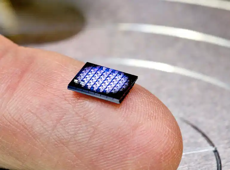
Nano assemblers are composed of nanoparticles and the first effect of reducing the size of the particles is to increase the surface area, the increase in the ratio of the surface area to the volume of nanoparticles causes that the atoms located on the surface have a much greater effect than the atoms inside the volume of the particles on the physical properties of the particles. Have. This feature greatly increases the reactivity of nanoparticles.The structure of nano assemblers is one of the properties of nanoparticles with a high surface to volume ratio of these materials. Using this property, powerful catalysts can be produced in nanometer terms. These nanocatalysts will greatly increase the efficiency of chemical reactions and also significantly prevent the production of waste materials in reactions. Nanoparticles in the production of other materials can increase their strength or reduce their weight. Increase their chemical and thermal resistance and change their reaction to light and other radiations. By using nanoparticles, the ratio of strength to weight of composite materials will increase greatly.

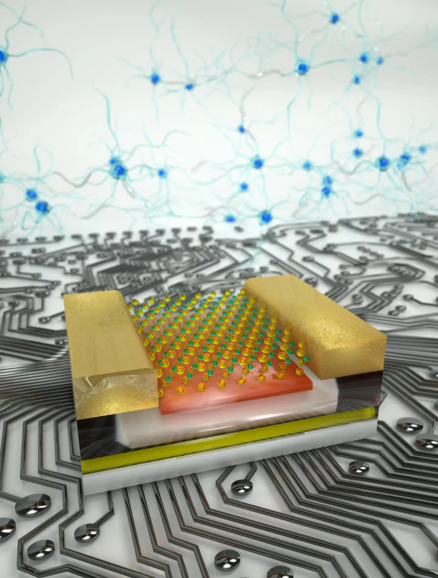
These devices, which include transistors and diodes, can be used in nanometer robots, nanoelectromechanical systems (NEMS), microelectromechanical systems (MEMS), and microfluidic devices. The mechanical action required to initiate deformation can be the pressing of a key, the pressure caused by the passage of a fluid, the stretching of muscles, or the movement of a robot's limbs.
Note: In smart nano-structures, the concept of Nano -assemblies is summed up in all the information and codes necessary to produce something similar to itself. We have a very small machine that knows how to produce something similar to itself , which is interpreted as a "nano-assembler" in nanoscience. will be
Nano assemblers are composed of nanoparticles and the first effect of reducing the size of the particles is to increase the surface area, the increase in the ratio of the surface area to the volume of nanoparticles causes that the atoms located on the surface have a much greater effect than the atoms inside the volume of the particles on the physical properties of the particles. Have. This feature greatly increases the reactivity of nanoparticles.
The structure of nano assemblers is one of the properties of nanoparticles with a high surface to volume ratio of these materials. Using this property, powerful catalysts can be produced in nanometer terms. These nanocatalysts will greatly increase the efficiency of chemical reactions and also significantly prevent the production of waste materials in reactions. Nanoparticles in the production of other materials can increase their strength or reduce their weight. Increase their chemical and thermal resistance and change their reaction to light and other radiations. By using nanoparticles, the ratio of strength to weight of composite materials will increase greatly.These devices, which include transistors and diodes, can be used in nanometer robots, nanoelectromechanical systems (NEMS), microelectromechanical systems (MEMS), and microfluidic devices. The mechanical action required to initiate deformation can be the pressing of a key, the pressure caused by the passage of a fluid, the stretching of muscles, or the movement of a robot's limbs.
Note: Compounds (III-V) The main factor in nanomaterials such as nano-emitting diodes to determine this spectrum is the energy gap in the semiconductor used.
To change the energy gap, there is no choice but to use semiconductor compounds instead of semiconductor elements. Decades ago, LEDs were still made with two spectrums of red and green light, but the possibility of making high-brightness blue nano-LEDs remained an unsolved mystery. Production of LEDs with blue light spectrum By GaN, it was possible to produce white light with LEDs. Part of the light the most efficient nano LED bulbs are increasingly finding wider application. Optical detectors are key components of these circuits. The main substrate for making these circuits is the photon crystal. Compounds (III-V) of nano-optical and nano-optical devices are among the most common applications of nano-microelectronics. Possibility of connection between silicon processor cores and external memory By integrated optical communication channels made of composite semiconductors, with a very high data transfer rate in other communication technologies and interconnection between processors, it has attracted the integrated optical nanoelectronics.
III-V Compounds Apart from some elements of group 4 of the periodic table, namely Si and Ge, which are semiconductors, compounds of elements of groups 3 to 5, group 2 to 6, as well as group 4 to 4 alloys also have semiconductor properties. Even some compounds of the three elements of these groups, such as AlGaAs and InGaN, have semiconductor properties . At the beginning of the study and research on these compounds, it was thought that they would soon replace silicon, because the possibility of engineering and obtaining some properties It did not exist in silicon, it was possible for them. However, due to the lack of suitable insulation for use in transistor gates, as well as the high cost of the elements and the coating process of V-III composite semiconductors, silicon and finally silicon-germanium alloy remain the main semiconductor.It should be noted that silicon oxide, which is easily layered with high purity, is a very good insulator for this purpose. Nowadays, in integrated circuits with a channel length below 50 nm, alternative oxides with higher dielectric coefficients, such as zirconium oxide ZrO2 and hafnium oxide, are obtained. He started. For example, in xAs-AlxGa1 and xN-InxGa1, a change in x leads to a change in the energy gap, and many of the properties of these semiconductor composites lead to the energy of the structural strip. Compounds (III-V) find nano-optical devices (xAs-AlxGa1) in (x <45.0 mode) along with changes in the distance between the edge of the capacity strip and the edge of the conduction strip by changing x in three different directions of wave propagation.