افشین رشید
اُستادیار ؛ عضو هیات علمی دانشگاه آزاد اسلامی واحد علوم و تحقیقات تهران
651 یادداشت منتشر شدهNano wire immersion method (structure and function)
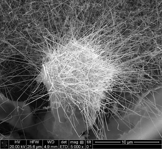
Note: In the immersion method, nanowires have enough time to transfer from nanoparticle particles to cavities ; The formation step of uniform nanoparticles is done slowly and finally uniform nanowires are formed.
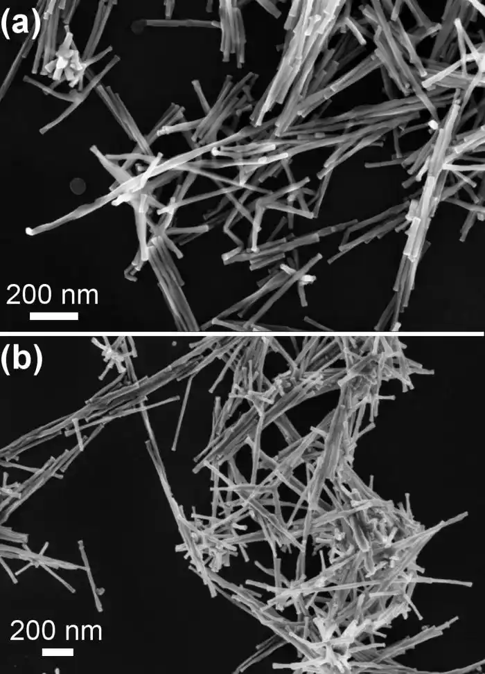
Structural study with FESEM in the immersion method of single-stranded nanowires in all porosities and in a large area of nanowire particles are formed. Changing the Sr / Fe ratio does not change the morphology of the nanowires. And spectroscopy of nanowires with a ratio of Sr / Fe states within the nano-particles inside (nanowires uniform) elements Fe and Sr of ferrite strontium in spectroscopy nanowires uniform is seen in the sample of nanoparticles Sr / Fe to value Its stoichiometry is closer to that of nanoparticles in electromagnetic composition, while due to the lower solubility of uniform strontium nanowire nanomolecules compared to iron nitrate and the consequent presence of less strontium ions in reaction with electromagnetic nanoparticles. There is more Fe ion in the final structure. Electro-magnetically active particles are used to separate uniform nanowires at ambient temperature . In the application of nanowires in nanoscale electronics or some other applications, it is necessary to separate the nanowires from alumina particles .

It is also necessary to separate the uniform nano-wires for better nano-electrostatic studies. In the application of uniform ferrite nanowires as microwave absorbers, it is not necessary to separate the nanowires from the inactive electromagnetic nanoparticles because the presence of an electrode material in the absorption of the ripple wave. Silicon nanowires are one of the best examples of semiconductor nanostructures that can be made in single crystals with a small diameter of 9 to 0 nanometers.
Electromagnetic nature of nanoparticles The magnetic material, molecules and atoms that make it up have electromagnetic properties. Simply put, elements such as iron, cobalt, nickel and their alloys are absorbed by the magnet . It is called magnetic material. The classification of electromagnetic materials is based on the magnetic susceptibility (magnetic capacity of the material). Based on this, materials are classified into three groups: ferromagnetic, paramagnetic and diamagnetic. The result of bipolar torque in electromagnetic diamagnetic materials is zero, and in the presence of a magnetic field, bipolar torque is induced in them; But for these two poles The induction is opposite to the direction of the external magnetic field, which causes a substance (diamagnetic) to be expelled from the magnetic field. By removing the external magnetic field, the magnetic properties of these materials do not remain. The magnetic susceptibility of these materials is very low (about 6-10 -3-10). All gases (except oxygen) are water, silver, gold, copper, diamonds, graphite, bismuth, and many organic compounds ( diamagnets). The magnetic dipoles in the paramagnetic material do not have a definite and regular orientation; As a result, these materials have no magnetic properties. If they are placed inside a magnetic field, they are aligned along the lines of the magnetic field. With the removal of the magnetic field , the magnetic dipoles quickly return to their previous state in the absence of the field. In this way, paramagnetic materials acquire strong magnetic properties in nano-electromagnetic fields.Nanowires have a structure that has an amazing length to width ratio . Nanowires are very thin - it is possible to create nanowires with a diameter of only one nanometer, nanowires are used to create the smallest transistors (nanotransistors). Nano wire Nano wire can have insulating, semiconductor or metal properties . Insulators do not withstand electrical charges, while metals have very good electrical charges. The semiconductors are located between the two and are charged under suitable conditions. By placing the semiconductor wires in the proper configuration, transistors can be made that act either as switches or amplifiers .Some interesting and anti-flexible features of nanowires are due to their small scale.
Note: Nanowires are used in the manufacture of computer nanoparticles that use light instead of electricity to create high computational speeds.
Making nanocomputers that use light instead of electricity to create high computational speeds . In military cases, biologically diagnosing cancers and other complex diseases with just a drop of blood, improving and modifying smart cards ; Used nano military drones and drones. Another nanostructure that has been studied and researched today is nanowires. A wire is generally a structure that extends in one direction (longitudinal direction) and is very limited in the other two directions . An essential feature of these structures, which have two outputs, is electrical conductivity. Electrical charge transfer occurs by applying a difference in electrical potential at both ends of these structures and along their length. Making wires in nanometer dimensions is very interesting both technologically and scientifically, because in nanometer dimensions, they have unusual properties . The ratio of length to diameter of nanowires is very high.
Examples of the use of nanowires are:
- Magnetic devices,
Chemical and biological sensors,
Biological markers and internal connections in nanoelectronics, such as the connection of two pieces of aluminum superconductor made by silver nanowires .
Types of nanowires:
Metal nanowires: These nanostructures promise great performance in electronic components due to their special properties. Metal nanowires are one of the most attractive materials due to their unique properties that lead to their various applications . Nanowires can be used in computers and other computing devices. To achieve complex nanoscale electronic components, we need nanoscale wires. In addition, nanowires themselves can be the basis of electronic components such as memory.
Use of nanowires in nano biological processors
Organic nanowires: These types of nanowires, as their name implies, are derived from organic compounds. In addition to metallic and semiconductor materials, nanowires can also be made from organic materials. Recently, a substance called "oligophenylene vinyl" has been developed for this purpose. The characteristics of these wires (such as conductivity and resistance and thermal conductivity) depend on the structure of the monomer and its arrangement.
Conductor and semiconductor nanowires in the propagation of nanochips: The chemical structure of these compounds produces interesting properties. The future of nanotechnology depends on the ability of researchers to acquire techniques for organizing molecular components and nanometer structures. By imitating nature, they organize the dough proteins to produce conductive nanowires. Organizing living components in nature is the best and oldest example of "bottom-up" construction, and therefore it can be used to understand and find ways to make electronic and micrometer devices. Until now, "top-down" manufacturing techniques have been used, which are often laborious and costly at the nanometer scale, and the commercialization of nanotechnology requires easy and cost-effective methods that best Its pattern is the nature around us; All we have to do is open our eyes a little and look around more carefully. Silicon nanowires: These types of nanowires are non-toxic and do not damage cells. This type of nanowires has shown its greatest application in medicine, such as detecting the symptoms of cancer, stem cell growth, etc. , which we will discuss below.
Application of nanowires in disease diagnosis and structure (nano _ bio chip) : Nanowires made from materials used in today's computer chips such as silicon and gallium nitride can be used to diagnose diseases. You may ask what computer tools have to do with the diagnosis of disease and the human body . The human body, like a computer, must have sensors that can warn of external warning devices in the event of a problem or error or the presence of toxic substances, such as A computer that gives an ERROR message if you run it in the wrong direction or a virus is found. Produce flexible, long nanowires with variable lengths ranging from 1 to 100 nm or even atIt is millimeters and is about a thousand times thinner than human hair in comparison. The height, flexibility and strength of these nanowires give it special properties. For example, being thin and long increases its surface area. Therefore, these structures can be used in the design of very fast and sensitive sensors. These nanowires have the ability to produce invisible ultraviolet rays, light enters the nanowire from one end and begins to shine from the other end. Nanowires pass this light efficiently without any loss. And in its path, if it encounters a pathogen or a toxic substance, the nanowire starts to shine and creates a very fast warning system , which can detect the disease sooner and faster than any test.
Using nanowires to make nanobots in blood vessels to stimulate the nerves of the brain: Always carry small transmitters into the arteries and direct them to the desired locations. Create platinum nanowires that are 100 times thinner and finer than human hair. They send these nanowires into blood vessels and direct them to the nerves of the brain through a small camera. This method is very useful to help find the various causes and emergence of neurological diseases, including Parkinson's. In the past, to find the various causes of heart and neurological diseases, the body was dug anywhere to find the cause of the disease, but today A device can be delicately, thinly and sensitively invented and even sent into the most delicate vessel.